banner

Solar wafer

Home

Solar wafer

N-type Boron diffused wafer

SE Process

N-type Boron diffused wafer

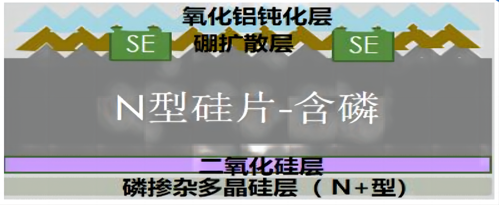
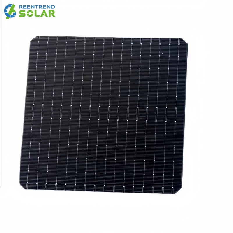
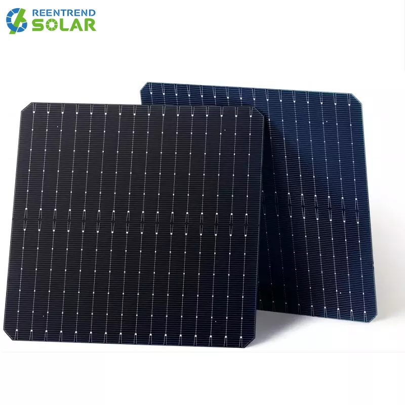
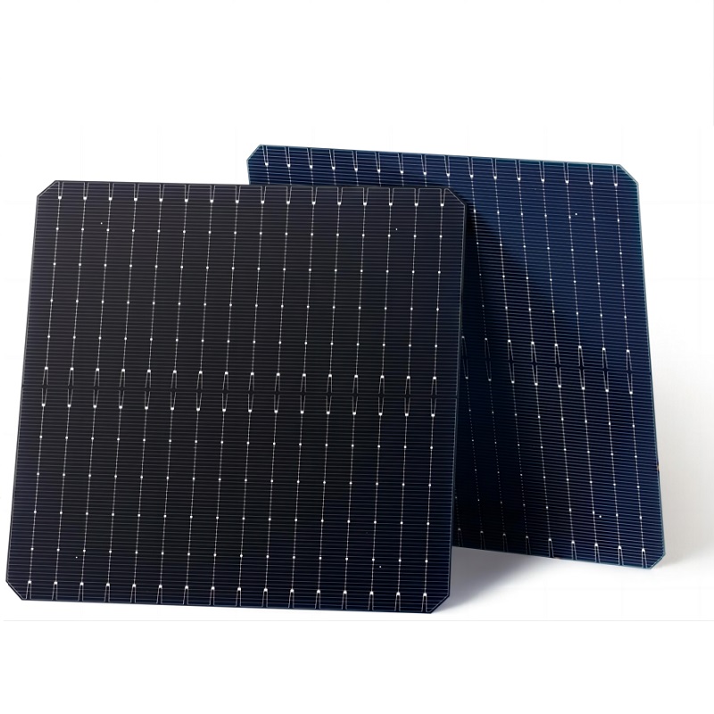
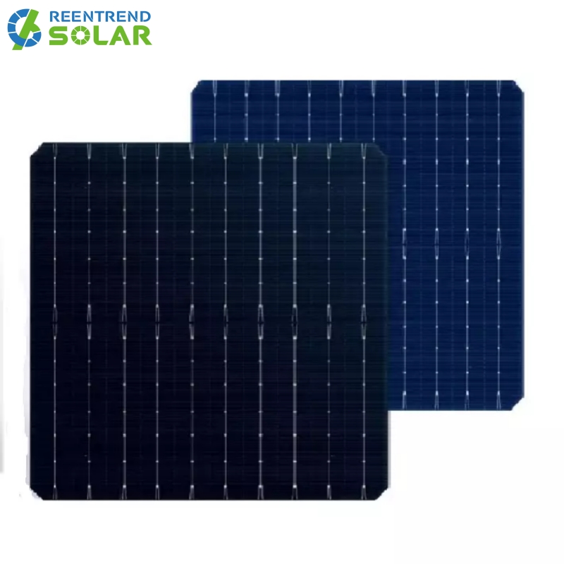
What is TOPCon Technology?


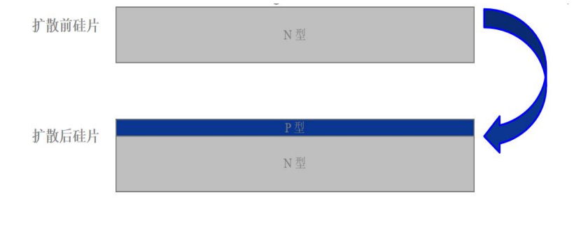
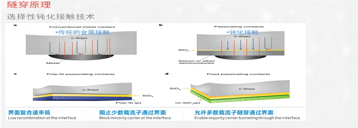
   The full name of TOPCON is Tunnel Oxide Passivating Contacts,  which is an N-type silicon wafer cell technology. TOPCon cells, namely tunneled oxide passivation contact solar cells, aim to improve solar cell efficiency by solving the problem of passivation contact of cell carrier selection.

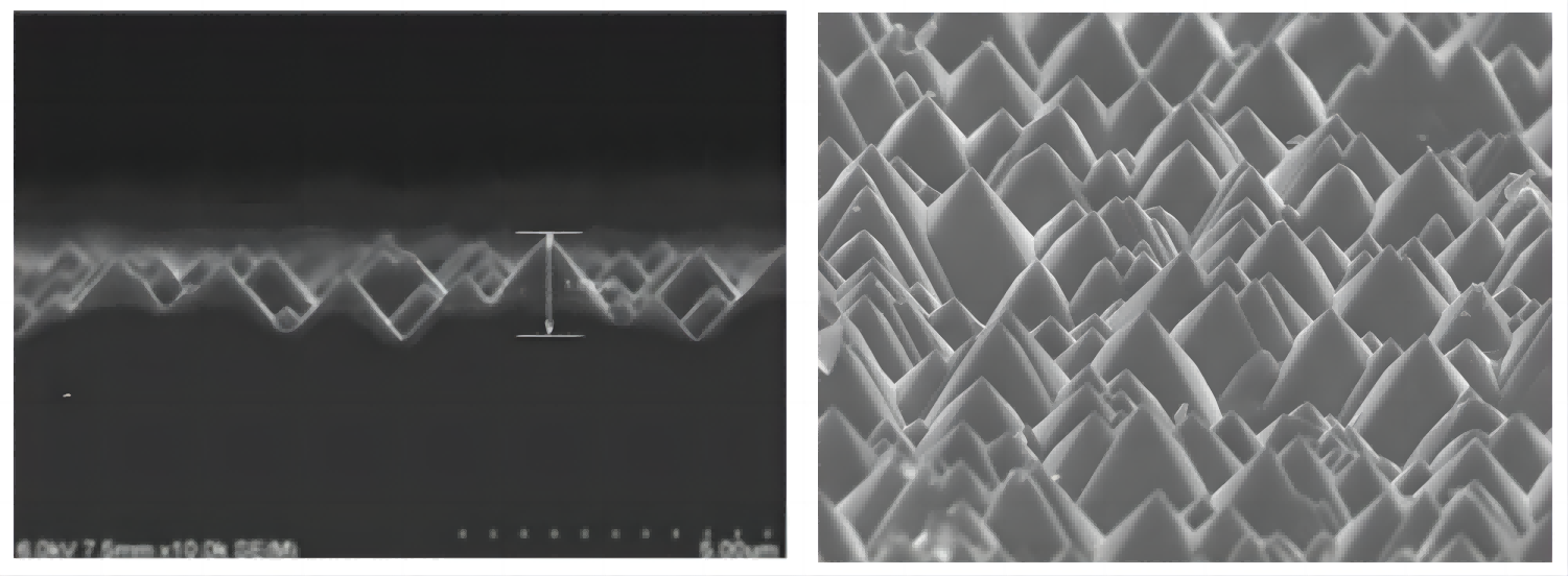
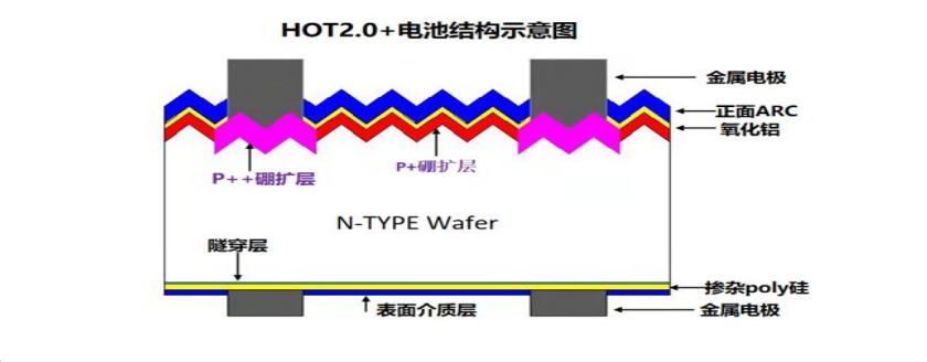
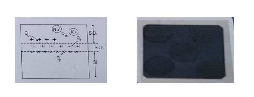
    The front surface of TOPCON cell has the same structure as that of conventional N-type solar cells, the main difference is to prepare a layer of ultra-thin silicon oxide on the back of the battery, and then deposit a thin layer of doped silicon, which together form a passivation contact structure, effectively reducing surface composite and metal contact composite.

    Due to the good passivation effect of ultra-thin silicon oxide and heavy doped silicon film, the surface band of the silicon wafer is bent, thereby forming a field passivation effect, the probability of electron tunneling is greatly increased, the contact resistance is reduced, and the conversion efficiency is finally improved.
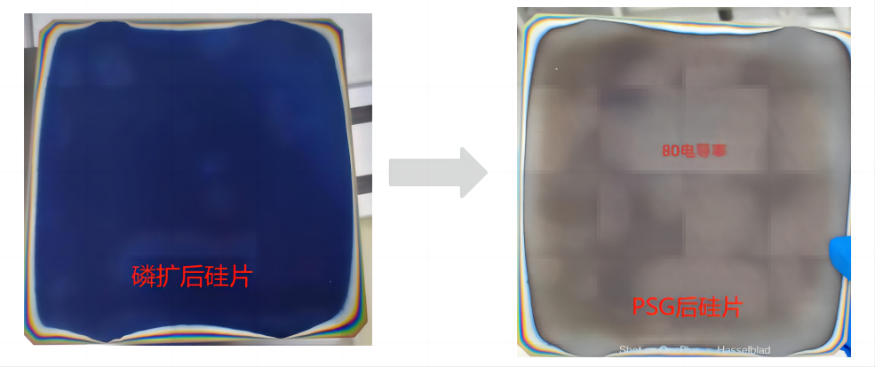
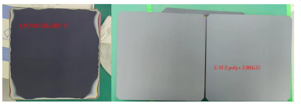
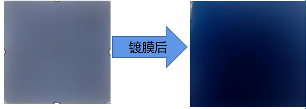
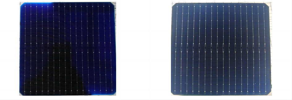
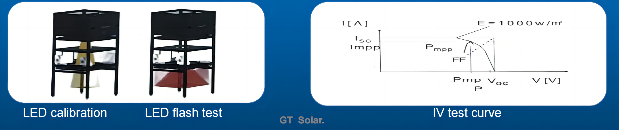
Our TOPCon process


Texture


Process introduction:The use of low concentration alkali solution has different corrosion rates on different crystal faces (anisotropiccorrosion), that is, the corrosion rate ratio of (100) faces (111) Fast surface, corrosion on the surface of the silicon wafer to form a corner cone (pyramid) dense surface topography, to increase the role of light incidence.
 
Boron Diffusion
Process introduction:The PN junction is formed by thermal diffusion method, and the boron trichloride impurity source is fully decomposed in the hightemperature diffusion reactor to produce silica and boron oxide
atoms, and the P-type boron impurity is driven into the N-type substrate at high temperature to form PN junction.
SE Laser
Process introduction:Selective emitter solar cells are doped with high concentration of boron impurities at and near the contact position between the metal gate line and the silicon wafer by laser doping, while
low concentration doping is formed in the area outside the electrode contact position, which reduces the contact resistance between the emitter and the electrode. The surface recombination is also reduced by the high resistance of light doped zone
Oxidation
Process introduction:The high temperature reaction in oxygen environment generates a dense boron-containing silicon oxide layer, which aims to activate boron atoms, increase effective doping, reduce interface recombination, and enhance boron impurity activity.
BSG
Process introduction:The BSG process consists of a process tank, a water tank, a drying tank and a loading and unloading table. The HF tank is first used to remove the borosilicate glass on the edges and back. The purpose is to prepare for the subsequent polishing process.
Rear side Etching
Process introduction:The alkali back etching process uses alkali and polishing additives for polishing. The purpose is to etch away the edge P-N junction and polish the back side. After alkali polishing, a surface with higher reflectivity can be obtained on the back side of the silicon wafer, which is beneficial to improving the back passivation performance. . After alkali polishing, thereflectivity of the backside is high, the specific surface area is small, the transmission loss is reduced, the recombination rate on the backside is reduced, and the output current and minority carrier lifetime are increased, thereby improving the solar cell conversion efficiency
LPCVD
Process introduction:An ultra-thin tunnel oxide layer and poly layer are grown on the rear side to provide good interface passivation and different carrier tunneling barriers. A layer of poly silicon is pyrolytically deposited on the tunnel layer to form tunnel oxide. Silicon passivated contacts have superior interface passivation and carrier transport capabilities.
Phosphorous Diffusion
Process introduction:The thermal diffusion method is used to form heavily doped n-type poly silicon, and the phosphorus oxychloride impurity source is fully decomposed in a high-temperature diffusion
reactor under high-temperature conditions to produce silicon dioxide and phosphorus pentoxide on the back poly silicon. The n-type phosphorus impurity is driven in at high temperature to form n-type heavily doped poly silicon.
PSG
Process introduction:The PSG process consists of a process tank, a water tank, a drying tank and a loading and unloading table. The HF tank is first used to remove the phosphosilicate glass on the edges and
front. The purpose is to prepare for the subsequent front-side etching process.
Front Side Etching
Process introduction:In the alkali front etching process, alkali is used with a curvature removal additive to perform poly etching on the four sides and sides of the front. The BSG/PSG layer on the front and back uses a curvature removal additive to form a barrier layer to prevent the reaction between BSG/PSG and alkali and protect the front boron expanded emission. The n+poly silicon on the front side and the back side are cleaned by acid and alkali in the functional tank to form a clean interface between the front emitter and the back side poly silicon.
ALD
Process introduction:Using atomic layer ylaluminum) reacts with deionized water to form an Al2O3 film, which has excellent passivation performance for boron expanded emitters, reduces interface recombination, and improves passivation performance. ALD has filmforming quality High efficiency, good uniformity, and precise control of film thickness. deposition, TMA (trimethylaluminum) reacts with deionized water to form an Al2O3 film, which has excellent passivation performance for boron expanded emitters, reduces interface recombination, and improves passivation performance. ALD has filmforming quality High efficiency, good uniformity, and precise control of film thickness.
PECVD
Process introduction:Plasma-enhanced chemical vapor deposition is used to drive the silane, ammonia and laughing gas to be ionized through external conditions such as low pressure, high temperature, and radio frequency excitation. The ionized reactants are deposited on the front/back to form a silicon nitride film. In order to play the role of anti-reflection, H ions will passivate dangling bonds, reduce recombination, and also play the role of interface passivation.
PRINTING&FIREING
Process introduction:The main purpose of printing & sintering is to prepare fine conductive lines on the surface of the solar cell, collect photogenerated carriers and conduct them out of the cell to form the positive and negative electrodes of the solar cell. The conductive paste will be designed under the action of the scraper and screen. The grid line pattern is transferred to the front and back through the screen, and then through high-temperature rapid sintering, the conductive paste printed on the front and back forms a silver-silicon alloy contact under the action of high temperature, so that the electrode and the emitter are in contact with each other. Poly-doped silicon forms excellent ohmic contact, as well as small metal contact area recombination.
Light Injection
Process introduction:A combination of LED light sources with a specific spectrum is used to illuminate the sintered solar cells. Through the effects of temperature and light intensity, the changes in the Fermi level are adjusted, and the total amount and valence state of H are controlled to improve the effect of H on internal defects and damage to the solar cells. Interface passivation performance.
 
TESTING&SORTING
Process introduction:By irradiating the surface of the solar cell with simulated sunlight, a photocurrent is generated. The photocurrent flows through the simulated load and generates a voltage at both ends of the load. The load device calculates the various properties of the solar cell through a series of calculations and corrections based on the collected current and voltage. index. Solar cells are sorted according to their photoelectric conversion efficiency, color, appearance and EL.
leave a message
If you are interested in our products and want to know more details,please leave a message here,we will reply you as soon as we can.

Related Products

leave a message

leave a message
If you are interested in our products and want to know more details,please leave a message here,we will reply you as soon as we can.
submit

Home

products

whatsApp

contact