In the past three to five years, the photovoltaic industry's solar cell technology has been rapidly upgraded and iterated, and high-efficiency PERC solar cells have gradually replaced traditional all-aluminum back-field solar cells and become a new generation of "conventional" solar cells. So, after PERC, where will the next PV technology outlet go?
Passivation contact – another outlet for photovoltaic technology after PERC
In recent years, passivation contact technology has become a research hotspot in the industry. The TunnelOxide Passivated Contact (TOPCon) technology developed by the Fraunhofer Institute for Solar Energy Research (Fraunhofer ISE) in Germany is one of the passivation contacts.

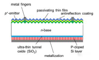
TOPCon solar cellstructure
TOPCon technology prepares an ultra-thin tunneling oxide layer and a thin layer of highly doped polysilicon on the back of the battery, which together form a passivation contact structure. The TopCon structure does not require backside holes and alignment, nor does it require additional local doping process, which greatly simplifies the solar cellproduction process. And it is well compatible with the current mass production process, which is convenient for production line upgrades. At the same time, the good passivation characteristics of the doped polysilicon layer and the metal full contact structure on the back have room to further improve the conversion efficiency, which can make the mass production efficiency of N-type cells exceed 23%. Based on the TOPCon cell structure, Fraunhofer achieves a conversion efficiency of 25.7% on a 4cm2 FZ silicon wafer.
Metallization is one of the key elements for the commercialization of TOPCon structures. Currently, full-back metal contact is achieved in laboratory equipment by physical vapor deposition (PVD) technology, but this technology is not suitable for large-scale mass production. In order to commercialize this promising and efficient technology, it is essential to find the right solution using screen printing and sintering metallization.
The challenge of screen printing metallization pastes for TOPCon solar cells
Developing metallization pastes for polysilicon layer contact and minimizing metal-induced recombination rates is a challenging task for the main reasons: First, reducing metal-induced recombination rates is very demanding due to the properties of metal-semiconductor interactions. Secondly, the polysilicon layer, which plays an important role in the contact performance of the slurry, has a significant difference. Key factors affecting the properties of polysilicon surface slurries include:
1. The thickness of polysilicon
From the perspective of absorption rate, ultra-thin polysilicon layer is preferred, but its metal-induced loss is more serious. In screen printing and sintering metallization processes, thicker polysilicon layers are often more advantageous. As long as the polysilicon layer is located on the back of the cell, even if the film layer is slightly thicker, it is completely acceptable.
2. Doping concentration of polysilicon layer
In order for good contact between the metal and polysilicon, a sufficient doping concentration must be achieved. Surface resistivity is a valid measure of whether the polysilicon layer is doped in situ at the time of deposition or trans-doped after deposition. The typical surface resistivity of polysilicon layers is higher than that of traditional diffusion layers, but this is usually only possible with ultra-thin polysilicon layers.
3. Surface morphology
The substrate surface for polysilicon deposition can be either textured or smooth. Recent studies have shown that both types of surfaces have excellent J0.
4. High temperature resistance
Being able to withstand higher temperatures is one of the advantages of polysilicon. However, the metal-induced recombination rate on the surface of the polysilicon layer is also a temperature function and usually accelerates as the temperature increases.
5. Uniformity of polysilicon layers
The uniformity of polysilicon layers generally increases with increasing thickness. This has an impact on contact performance, as inhomogeneous polysilicon layers are prone to more severe localized damage during metallization.
It can be seen that the characteristics of polysilicon have a profound impact on the characteristics of the slurry. It is reported that metallization pastes with optimal contact resistance and minimized metal-induced recombination rates have been developed.
The latest progress of TOPCon solar cells and metallization pastes
In January 2019, JinkoSolar announced that its high-efficiency N-type monocrystalline TOPCon large-area solar cell conversion efficiency broke the world record, achieving a photoelectric conversion efficiency of 24.2% through the use of high-quality N-type monocrystalline silicon wafers, cell selective doping technology, and ultra-fine gate printing.
In February 2019, the Solar Energy Research Institute of Singapore (SERIS) and a leading domestic paste manufacturer signed a cooperation agreement to accelerate the development of metallized pastes for monoPoly™ passivated contact solar cells. SERIS expects the average efficiency of its monoPoly™ cells to increase to 23.5%-24.0% by using metallization pastes developed specifically for the technology.
As the largest N-type cell and module manufacturer in China, Jolywood is currently making every effort to upgrade its 2GW N-PERT cell production line to n-TOPCon cells. It is reported that Jolywood Optoelectronics has adopted screen printing metallization paste technology, and the average efficiency of TOPCon solar cellmass production has reached 22.6%. By optimizing the solar cellmanufacturing process, the average efficiency can be increased to more than 23%.