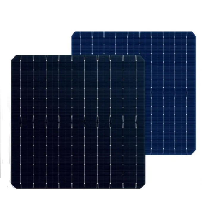
Laser processing is an important technology to reduce costs and increase efficiency of solar cells. It has obvious advantages over traditional technologies in the fields of PERC laser ablation, SE laser doping, repair and metallization; among them, PERC laser grooving, SE laser Doping is the application of laser marking technology to etch specific microstructures on the cells to achieve the purpose of improving photoelectric conversion efficiency. The processing accuracy is high and the speed is fast, and the scanning speed of the galvanometer is above 60m/s.
1. SE laser doping principle
1.1 Principle of doping
Selective emitter (SE) solar cells perform high-concentration doping at and near the contact area between the metal gate line and the silicon wafer, while low-concentration doping is performed in areas other than the electrodes.
1.2 Effect of emitter doping concentration on efficiency
High concentration doping:
Advantages: Reduce the contact resistance between the solar silicon wafer and the electrode, and reduce the series resistance of the solar cells;
Disadvantages: The carrier recombination becomes larger and the lifetime of minority carriers is reduced, which affects the open circuit voltage and short circuit current of the solar cells.
Low concentration doping:
Advantages: Reduce surface recombination and improve minority carrier lifetime;
Disadvantages: increased contact resistance, affecting the series resistance of the solar cells.
2. SE solar cells advantages
2.1 Reduce series resistance and increase fill factor
a. The series resistance of the solar cell consists of the grid line body resistance, the contact resistance between the front grid and the silicon surface, the diffusion layer sheet resistance, the silicon chip body resistance, the back electrode contact resistance and the back field body resistance.
b. According to the metal-semiconductor contact resistance theory, contact resistance is related to the metal barrier and surface doping concentration (Nd). The lower the barrier, the higher the doping concentration, and the smaller the contact resistance.
2.2 Reduce carrier recombination and improve surface passivation effect
a. When the impurity concentration is greater than 1017/cm-3, recombination is the main recombination mechanism in semiconductors, and the recombination rate is inversely proportional to the square of the impurity concentration. The shallow doping of SE can effectively reduce the lateral flow of carriers in the diffusion layer , improve the collection efficiency of carriers.
b. Low surface doping concentration means low surface state density and improved passivation effect.
2.3 Enhance the short-wave spectral response of the solar cells and increase the short-circuit current and open-circuit voltage
a. For AM1.5, about 20% of the energy of incident light is absorbed in the diffusion layer. Shallow diffusion can improve the quantum efficiency of these short-wavelength sunlight and increase the short-circuit current.
b. Due to the existence of a lateral (n++-n+) high and low junction, the open circuit voltage is increased.
2.4 Based on the following efficiency influencing factors, the final result can increase the efficiency by more than 0.2% compared with conventional solar cells.
3. The impact of emitter on solar cell conversion efficiency
3.1 Appropriately increase the sheet resistance to increase the open circuit voltage and short circuit current. However, in the screen printing method, the contact resistance between the Ag electrode and the low surface doping concentration emitter is relatively large. As a result, the conversion efficiency decreases due to the decrease in fill factor;
3.2 The n+ diffusion layer of traditional solar cells is generally 50-60Ω/sqr, while the shallow diffusion resistance of the SE structure is generally 100-110Ω/sqr, and the heavily doped resistance under the electrode is lower than 40Ω/sqr;
3.3 In order to simultaneously increase the open circuit voltage and short circuit current without reducing the fill factor, the selective emitter solar cells is heavily doped at the solar cells contact part and lightly doped at the position between the electrodes;
