

After purposeful doping, the semiconductor bulk silicon introduces trace impurities to become an extrinsic semiconductor, which is divided into N-type and P-type two categories.
1. N-type crystalline silicon
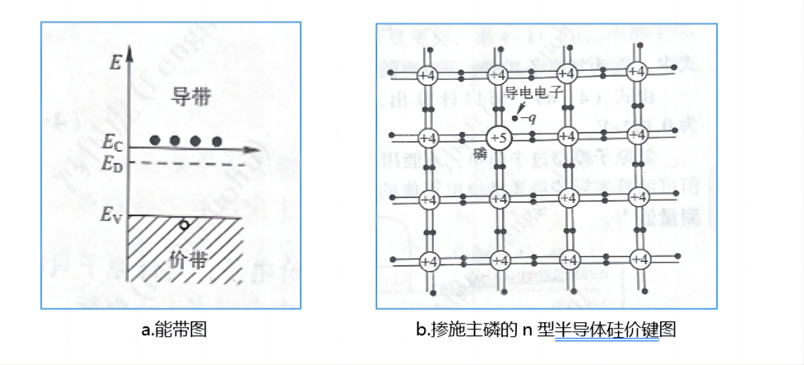
When the crystal silicon is mixed with trace impurities Group V elements, its five valence electrons form four covalent bonds with silicon atoms, Group V ion nuclei have a positive charge, forming a positive center, while also having a valence electron, this electron is bound by the positive center, forming a bound state electron, its energy level is below the bottom of the conduction band.
The diagram below shows the silicon valence bond diagram of N-type semiconductor doped with donor (phosphorus). As can be seen from the figure, when a silicon atom is replaced by a phosphorus atom, a group V element with five valence electrons, the phosphorus atom forms a covalent bond with its four neighboring silicon atoms, and the extra electron becomes a conductive electron.
When the electron gains energy and breaks free from the bond of the Group V impurity atom, it becomes an electron that can conduct electricity and forms a positive electric center. This impurity atom, which can release electrons to the conduction band to form a positive center, is called a donor. The phosphorous atom shown in the figure is the donor. Because the donor in silicon can provide electrons, electrons are negatively charged carriers, so the semiconductor silicon dominated by the donor in the impurity is called N-type semiconductor silicon.
2, P-type crystalline silicon
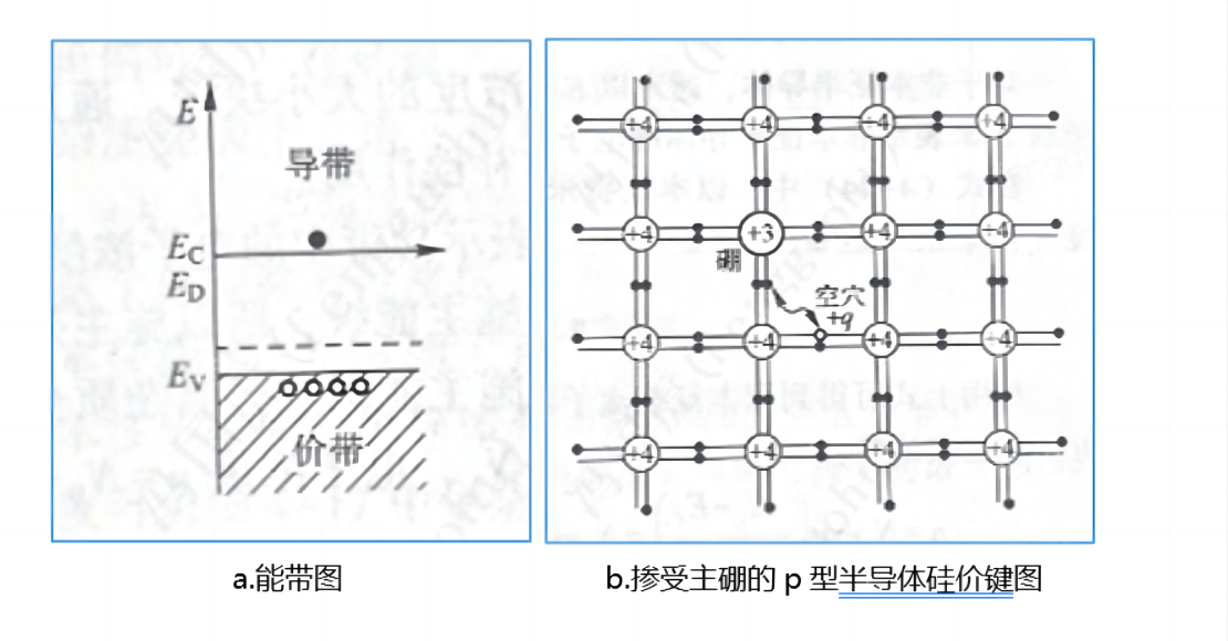
When a group III impurity atom is added to crystalline silicon, because it has only three valence electrons, it can only form three covalent bonds with silicon atoms, so a vacancy (called a hole) appears in the valence bond. The hole corresponds to a positive charge. The ionic nucleus of a group III atom has only three positive charges, forming a negative center in the lattice, which can bind holes.
As shown in the figure below, a boron atom with only three valence electrons replaces the silicon atom, and in forming four covalent bonds with the neighboring silicon atom, it needs to accept one electron, which creates a positively charged hole in the valence band. The group III impurity that forms a negative charge center can accept electrons in the valence band and form holes in the valence band, so it is called the acceptor impurity, and its energy level is called the acceptor energy level, and the group III impurity boron atom that can accept electrons shown in the figure is the acceptor.
Holes can be regarded as positively charged carriers. A semiconductor dominated by acceptors capable of forming positively charged carriers is called P-type semiconductor silicon.
3. Summary:
When pure silicon is mixed with donor impurities (V group elements phosphorus, arsenic, antimony), N-type silicon can be formed, the concentration of N-type silicon conductive electrons is much greater than the concentration of conductive holes, the current depends on electron transport, electrons are most carriers (referred to as many), holes are a few carriers (referred to as few).
When pure silicon is mixed with acceptor impurities (group III elements boron, aluminum, gallium), P-type silicon can be formed, P-type silicon hole concentration is much higher than the electron concentration, the current depends on the hole transport, the hole is many, the electron is few.


 English
 español
 한국의
한국의


 IPv6 network supported