HJT, short for Heterojunction Technology, is an N-type monocrystalline bifacial cell with the advantages of simple process, high power generation and low cost of electricity. HIT (Heterojunction with Intrinsic Thin layer) has been registered as a trademark by Sanyo Corporation of Japan, so it is also known as HJT or SHJ (Silicon Heterojunction). This type of solar cell was first successfully developed by Japan's Sanyo Corporation in 1990 with a conversion efficiency of 14.5% (4mm2 cells), and later with the continuous improvement of Sanyo Corporation, the conversion efficiency of Sanyo HJT cells reached 25.6% in 2015.
As shown in Figure 1, a thin intrinsic amorphous silicon film (i-a-Si:H) and a p-type amorphous silicon film (p-a-Si:H) are deposited on the front side of the N-type monocrystalline silicon wafer (c-Si), and then a thin intrinsic amorphous silicon film (i-a-Si:H) and n-type amorphous silicon film (n-a-Si:H) are deposited on the back side of the silicon wafer to form a back surface field. By depositing transparent conductive oxide (TCO) films on both sides of the cell through PVD, TCO can not only reduce the series resistance when collecting current, but also play a role in reducing reactions. Finally, the metal electrode is fabricated on the TCO.
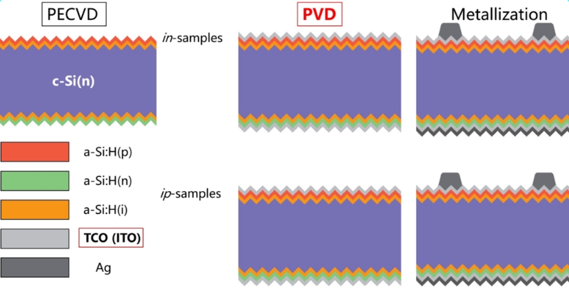 Fig.1 Schematic diagram of HJT solar cell structure
The following is an example of a common ITO.
1.Crystal structure of ITO films
Transparent conductive oxide film has the dual functions of optical transparency and conductivity, plays a key role in the collection of effective carriers, can reduce the reflection of light, plays a good role in light trapping, and is a good window layer material. Examples include zinc oxide (ZnO), indium oxide (In2O3), tin oxide (SnO2), F-doped tin oxide (FTO). At present, there are many studies on doped metal oxides based on In2O3, SnO2 or ZnO, especially tin-doped indium oxide (ITO) and aluminum-doped zinc oxide (AZO).
ITO thin film is a wide bandgap transparent conductive semiconductor, composed of III.A and VI.A oxides, indium oxide (In2O3) has 80 atoms in the unit cell, including 32 indium and 48 oxygen, the ratio is 2:3, the density is 7.12 g/cm3, its lattice constant is a=1.0117 nm, and the crystal structure is shown in Figure 2, in which indium atoms occupy the body center of the body-centered cube, six oxygen atoms occupy the apex angle of the body-centered cube, and the remaining apex corner position is oxygen vacancy. The doping of Sn (donor) in indium oxide is the substitution of the position of In in the crystal lattice. Indium tin oxide (ITO) is an n-type semiconductor, in which the tin content is generally 10%, and the ITO film is a semiconductor metal oxide transparent conductive film due to heavy doping. The carrier concentration of ITO film is about 1020 cm-3, and it has a high mobility of about 15~45 cm2V-1·s-1 and a conductivity of 104 Ω-1·cm-1. At the same time, ITO films have a large bandgap width of 3.5 ~ 4.3 eV, and their average transmittance in the visible band is greater than 80%.
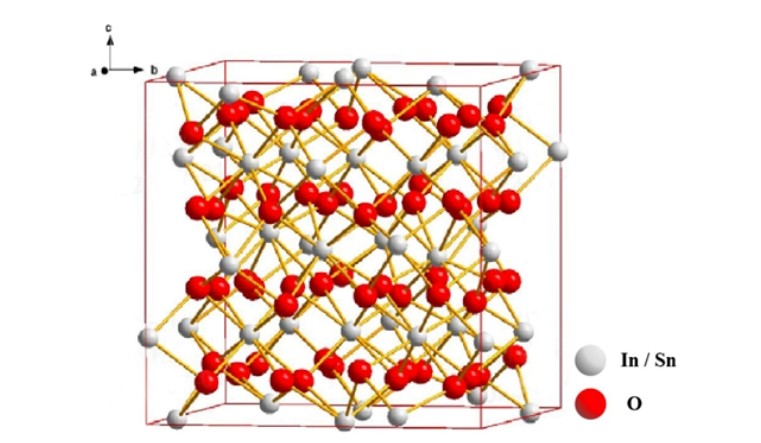
Fig.2 In,O, schematic diagram of crystal structure
Since ITO is a wide bandgap semiconductor, the bandgap width is greater than the photon energy of visible light, so when visible light irradiates the film, most of the photons will pass through; On the other hand, ITO's plasma wavelength is near-infrared, i.e., its plasma frequency is less than that of visible light, and therefore, its absorption and reflection of visible light is weak.
2.Electrical properties of ITO films
The conduction mechanism of indium oxide thin films is mainly due to two defects in the crystal structure, impurity defects and intrinsic defects. Among them, the impurity defect is caused by the doping of tin atoms in the crystal, while the intrinsic defect is mainly the oxygen deficiency. After the incorporation of SnO2, the Sn atom tends to be solid solution in the way of Sn4++4e, and the Sn4+ ion occupies the position of In3+ in the crystal lattice, in order to maintain electrical neutrality, the variable Sn4+ will capture an electron and become Sn4+·e, that is, Sn3+. The connection between this electron and Sn3+ is weakly bound and easy to lose, and this electron is the main source of carriers, and its conductivity is mainly affected by the electron concentration and electron mobility in the semiconductor, so the holes have almost no effect on the conductivity of n-type semiconductors. The conductivity σ is represented by equation (1),

g - Carrier charge; n - the amount of charge of the carrier; From a carrier of charge
As can be seen from the above formula, the conductivity of the material is mainly determined by the electron mobility and carrier concentration of the film. The movement of the carriers in the material is the result of the acceleration and continuous collision of the electric field, and the carriers in the ideal crystal are not hindered by external forces, but the various impurity defects in the actual crystal and the atomic vibration in the crystal will scatter the movement of the carriers. These scattering effects include impurity scattering, lattice scattering, grain boundary scattering, etc. The smaller the scattering effect, the faster the carrier movement speed and the greater the conductivity. On the contrary, the more obstacles encountered by the carriers in the motion, the more their motion is continuously blocked, the scattering effect is enhanced, the carrier velocity is reduced, and the conductivity of the film is smaller. In addition, when the oxygen vacancies formed in the preparation of ITO films are excited, they can provide two free electrons, which can also play a role in increasing the carrier concentration. ITO films typically have high conductivity due to the high carrier concentration (about 4×1020 cm-3) and electron mobility (40 cm2V-1·s-1) at the same time.
3.Optical properties of ITO films
The optical properties of transparent conductive films are an important indicator of whether they can be applied in practice. The transmittance of the film is closely related to its band gap. The band gap refers to the part of the lattice periodic potential field that cannot be valued, that is, the area where the value of the forbidden energy exists. When a transparent conductive film is irradiated by light, the low-energy electrons in it will transition due to the energy they get, forming electron-hole pairs to complete the absorption of photons, and the band gap width will have a great impact on the optical properties of the semiconductor. The band gap width mainly depends on the atomic composition and bonding state in the film, but it is also affected by impurities and defects. Defects in the material and external doping can significantly alter the carrier concentration and thus affect the band gap of the material. This is shown in Figure 3. Eg and Eg' represent the bandgap widths of In2O3 and ITO respectively, and the actual optical bandgap of ITO films is usually larger than that of undoped In2O3. Therefore, ITO's wide optical bandgap is a necessary condition for its use as a high-transmittance thin film material. The change of temperature also has a certain effect on the transmittance of the ITO film, which is already high at room temperature, and the transmittance of the ITO film at the wavelength of 550 nm is more than 90%. When the substrate temperature is 200°C, the transmittance of ITO films increases slightly, mainly due to the reduction of the SnO phase in ITO films, and the ITO films deposited at 200°C are polycrystalline, and the lattice defects in the film have less effect on the scattering of photons, which can also increase the optical transmittance of ITO films, as shown in Figure 4.
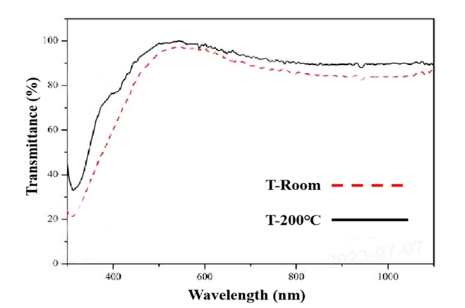
Fig.3 Schematic diagram of the bandgap widths of In, 0 and ITO
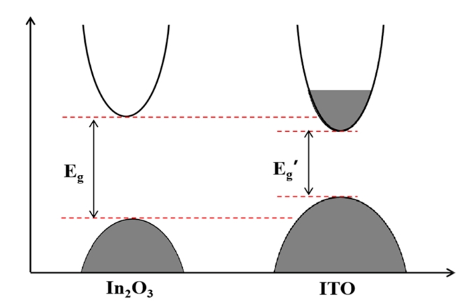
Fig.4 Schematic diagram of the bandgap widths of In, o., and ITO
Since the band gap of In2O3 > 3.5 eV, and the average energy of visible photons is about 3.1 eV, it cannot cause intrinsic excitation under the irradiation of visible light, so it has a high transmittance in the visible light range. There are three main types of optical absorption processes of TCO, as shown in Figure 5, and the main optical absorption process of semiconductor materials is intrinsic absorption. In general, ITO has higher absorption in the short-wavelength region, higher reflectivity in the long-wavelength range, and the highest transmittance in the visible light range. In the case of a 100nm ITO, the average transmittance in the 400-900nm wavelength range is as high as ~90%.
Fig.5 Three types of light absorption processes in TCO
1 Intrinsic absorption
The energy of the electrons in the valence band is lower and the energy absorbed is lower
After measuring the photons ≥ the width of the band gap, the electron-hole pairs are generated by the transition from the valence zone to the conduction band, which completes the absorption of photons.
2 Exciton absorption
When a photon is irradiated at energy < half the width of the band gap
On the conductor material, the excited electrons and holes are bound to form excitons in a certain space under the influence of Coulomb force. This absorption
Accompanied by exciton generation
3 Impurity absorption
That is, the electrons and empty six in the impurity energy level are absorbed
After collecting the photon energy, it transitions to the conduction band energy level, and the hole can also absorb the energy of the photon, and the energy of the photon jumps to the valence band energy level, and this photon is absorbed
This is called impurity absorption
4.Electrical properties of ITO films
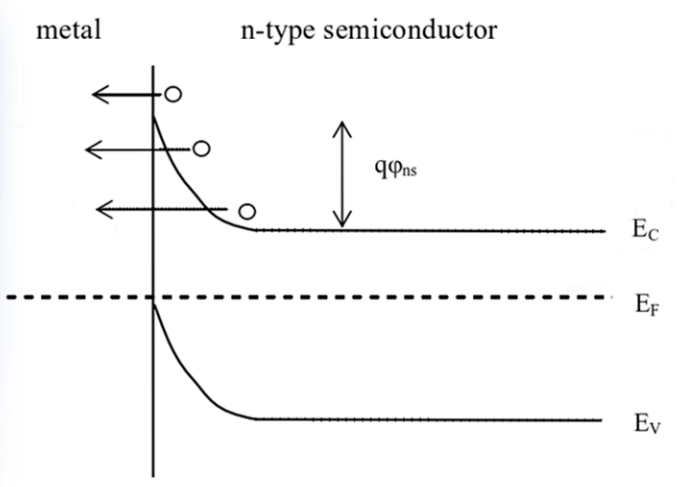
Whether ITO films are used as transparent electrodes or anti-reflective layers in silicon-based solar cells, they need to form good ohmic contact with silicon. That is, a special kind of metal (or TCO) contact with the semiconductor, the main feature is that the metal and the semiconductor contact presents a small resistance, ohmic contact usually shows that the contact between the metal and the semiconductor has linear I-V characteristics, and its voltage drop can be negligible. Different carrier transport mechanisms in metal-semiconductor Si contact. In the contact between the metal and the semiconductor Si, there are three main ways for the carriers to be transported from the semiconductor to the metal when the forward bias is positive: (1) the thermal electron emission mechanism: the electron crosses the top of the semiconductor barrier and thermally emits to the metal; (2) Field emission mechanism: the electrons in the conduction band of the semiconductor pass through the barrier and enter the metal with the quantum mechanical tunneling effect; (3) Thermal electron field emission mechanism: electrons with energy lower than the top of the barrier are excited by energy to a region with a low barrier height and a thin depletion layer, and have a certain chance of passing through the barrier in the form of tunneling effect. The transport mechanism of the carriers has a lot to do with the doping concentration of Si, and the different carrier transport mechanisms are shown in Figure 6 in the case of metals and n-type semiconductors. However, in the actual contact, the transport of carriers will not be completed by a single transport mechanism, so there is often a thermal-electron field emission mechanism in the thermal-electron emission mechanism, which makes the current in the contact different from the theoretical current of the thermal-electron emission mechanism. When the doping concentration of semiconductors is moderate, the emission of thermal electron field becomes the main mechanism of carrier transport.
5.Heterojunctions were prepared with TCO-PVD
The TCO films commonly used in HJT cells and have been industrialized are In2O3 series, such as ITO (tin-doped In2O3, commonly used by PVD magnetron sputtering), IWO (tungsten-doped In2O3, commonly used by RPD deposition), etc., and the process comparison of PVD and RPD is shown in Table 1.
Table 1 Comparison between PVD and RPD processes
PVD
Advantages
3. The sputtering process is repeatable, and the thickness is accurately controlled
4. Different metals, alloys, and oxides can be mixed and sputtered on the substrate at the same time
5.The equipment has a large capacity and a low comprehensive cost.
Disadvantage
3. The cost of target materials is high, and the supply of target materials is restricted by some foreign manufacturers
summary
It is more suitable for mass production
RPD
Advantage
Shortcoming
3. The process stability is poor, and it is not suitable for large-scale production