

What do "M" and "G" stand for in solar wafer size?
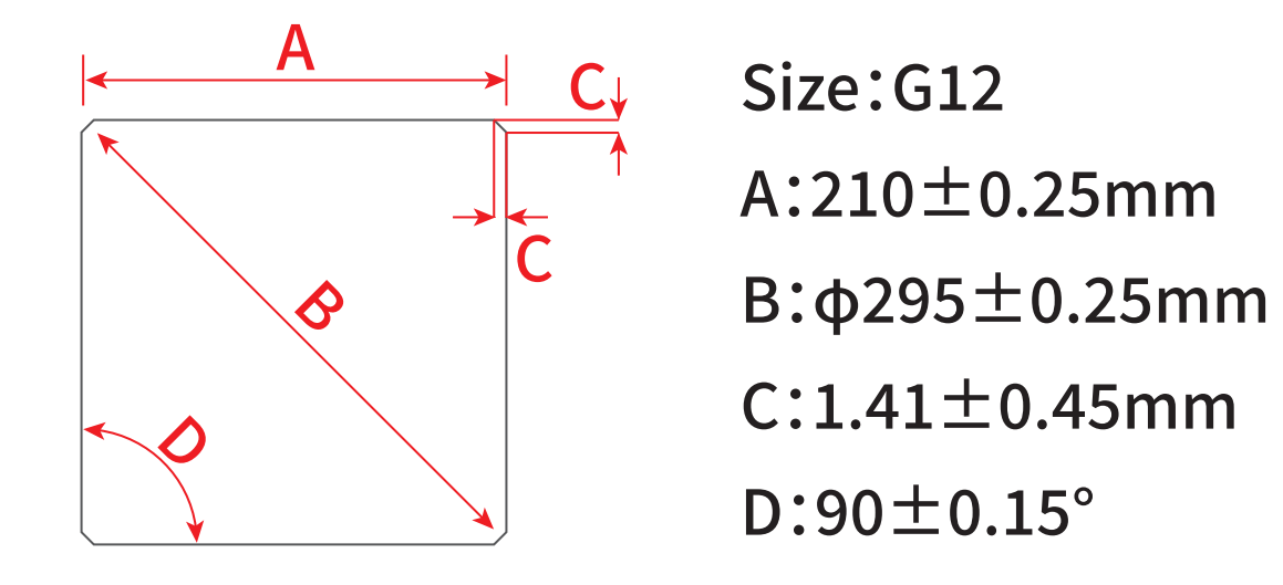
It begins with the letter "G", which means that the solar silicon wafer is full square
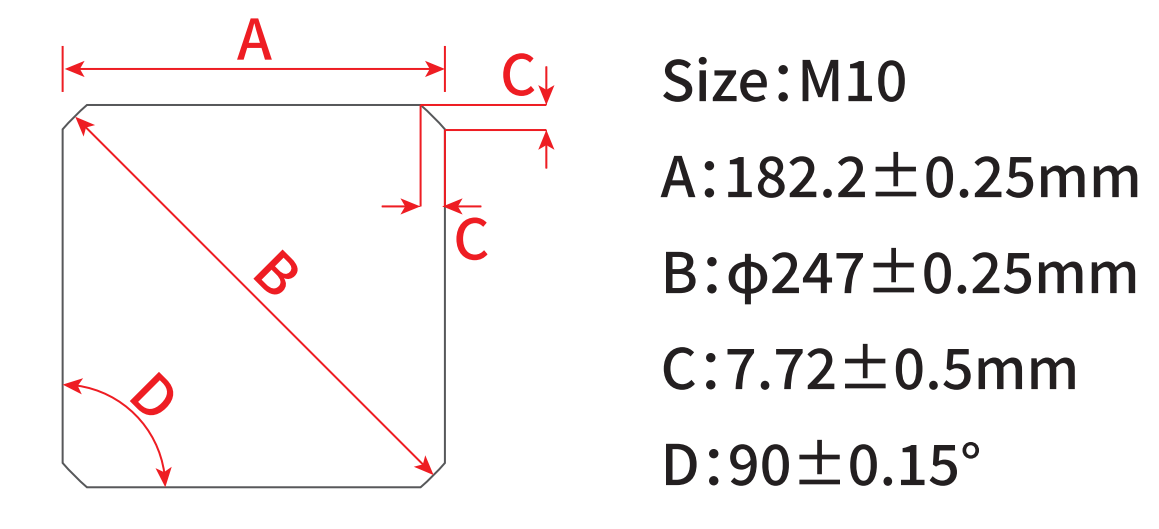
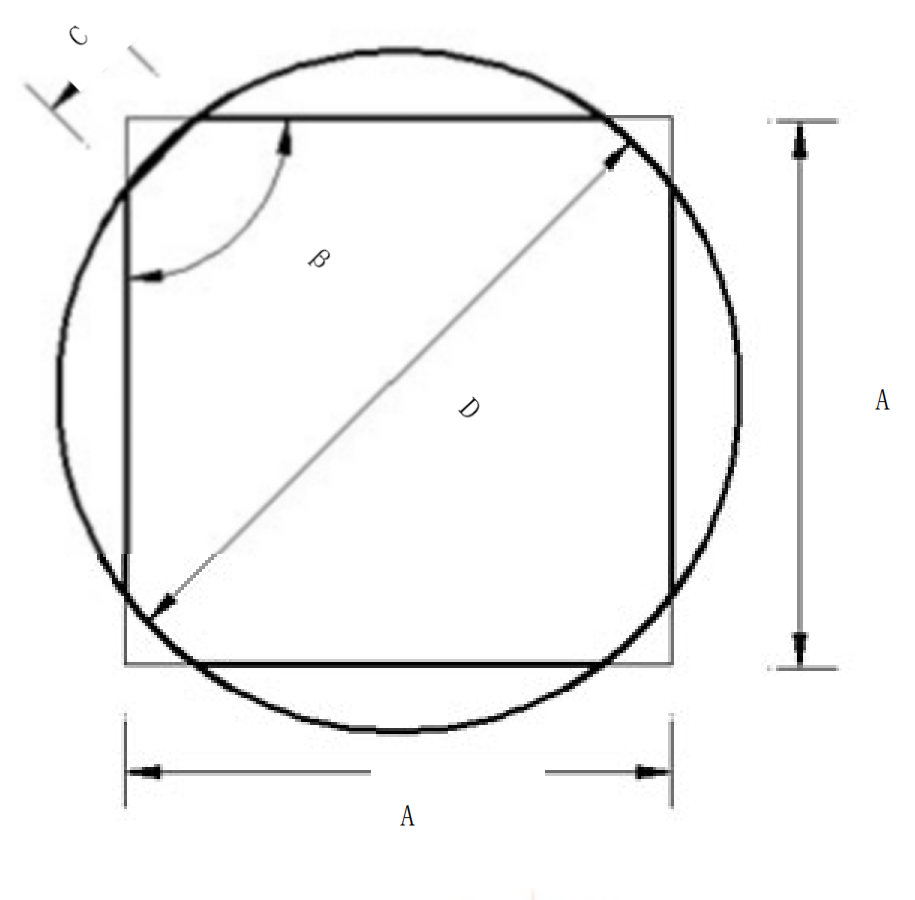
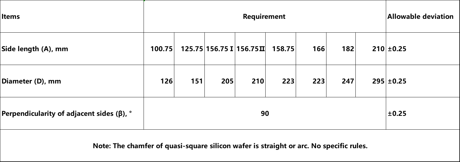
Beginning with the letter "M", it means that the solar silicon wafer is Pseudo-square and has chamfer.
EG:
As an important link in the upstream of the photovoltaic crystalline silicon industry chain, silicon wafers have always played a unique and irreplaceable role in cost reduction. Large size and thinning are two key directions for reducing cost and increasing efficiency of silicon wafers.
From the material point of view, silicon is divided into polysilicon and monocrystalline silicon, but with the conversion efficiency of monocrystalline silicon cells to become the mainstream of the market, polysilicon has been eliminated, at present, the photovoltaic industry for silicon wafer differentiation mainly lies in the size.
The silicon wafer size has undergone three major changes: the first stage from 1981 to 2012, the silicon wafer size is mainly 100mm, 125mm; The second stage from 2012 to 2015, mainly 156mm (M0), 156.75mm (M2); Since 2018, large size silicon wafers such as 158.75mm (G1), 161.7mm (M4), 166mm (M6), 182mm (M10),210mm (G12) and 210m*X(210R) have appeared
The geometry of solar silicon wafers
Geometric diagram of square silicon wafer
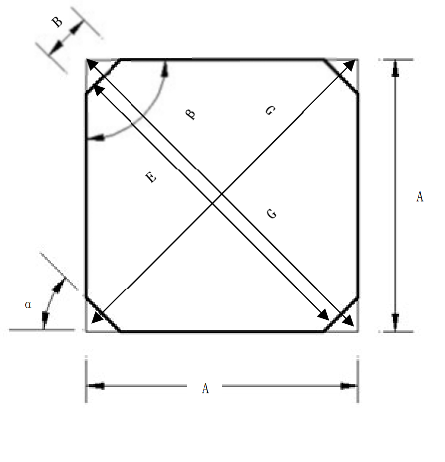
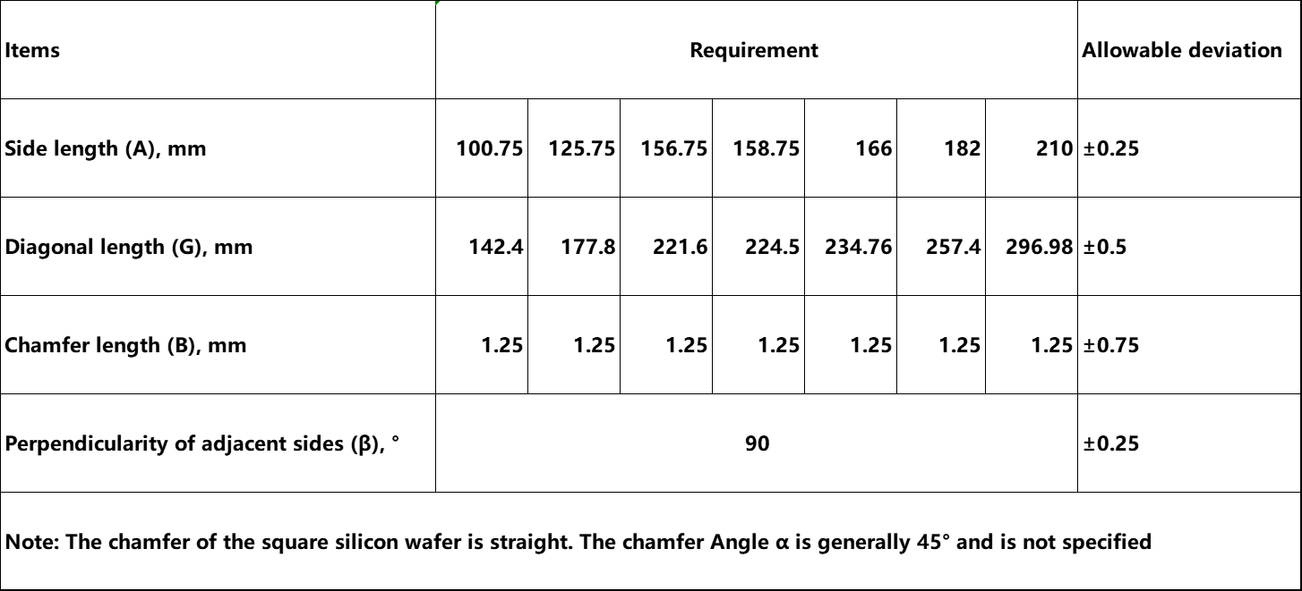
Geometric diagram of quasi-square silicon wafer
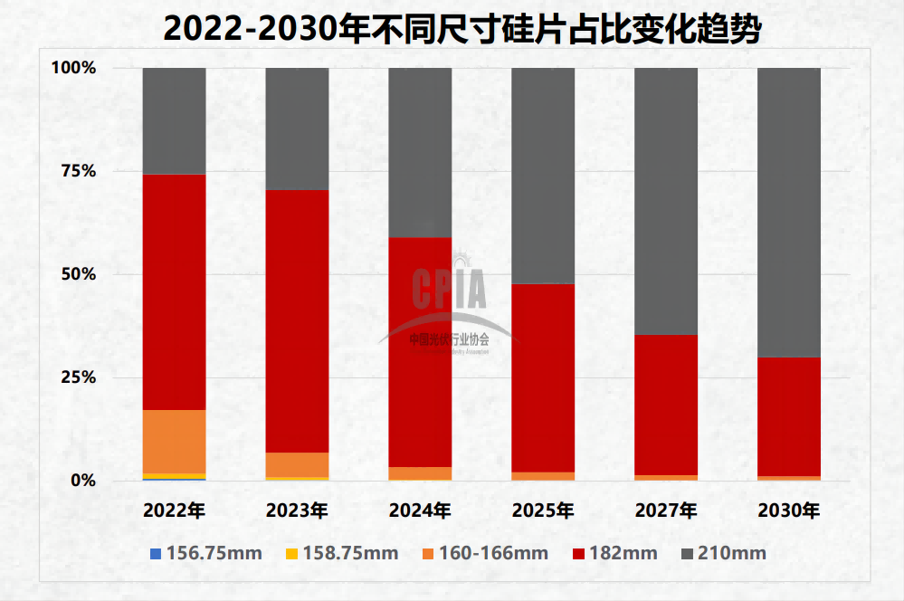
Large-size silicon technology refers to the use of large-size silicon wafers in the production of cells and modules, so as to reduce the loss in the energy conversion process, improve the efficiency of solar cells and module power. According to CPIA statistics, in 2022, there are various types of silicon wafer sizes on the market, including 156.75mm, 157mm, 158.75mm, 166mm, 182mm, 210mm, etc., and each occupies a certain market share.
In 2022, the combined market share of large-size silicon wafers represented by 182mm (M10) and 210mm (G12) has exceeded 80%.
Large size silicon wafers can reduce costs in both photovoltaic manufacturing and photovoltaic applications, thereby reducing the application cost of photovoltaic power generation.
In the aspect of manufacturing, increasing the size of silicon wafer is conducive to increasing the feeding amount of long crystal furnace and reducing the energy consumption. In the manufacturing process from rod, slice, cell to component, increasing the size of silicon wafer is conducive to increasing production capacity at a lower marginal cost, reducing labor costs and depreciation costs; In the component manufacturing process, increasing the size of the silicon wafer can reduce the connection between the cells, which is conducive to improving the reliability of the components, and reduce the gap area between the cells, improve the efficiency of the components, and thus improve the utilization efficiency of the components. All of these factors together reduce the non-silicon cost per watt of components. At the same time, increasing the size of the silicon wafer allows for the manufacture of higher-power components.
In terms of application, high-efficiency and high-power components can reduce the land area of the power station, improve the efficiency of land use, and reduce the BOS consumption of brackets and cables, reduce the manual installation of components, facilitate the maintenance of the power station, and thus reduce the construction and operation and maintenance costs of the power station, which is an effective way to reduce the levelized power cost of photovoltaic power stations.
According to CPIA data, the total proportion of large-size silicon wafers represented by G12 (210mm size) and M10 (182mm size) has rapidly increased from 4.5% in 2020 to 82.8% in 2022, becoming the absolute mainstream of the market.


 English
 español
 한국의
한국의


 IPv6 network supported