The efficiency of N-type polysilicon backside passivated contact (PSPC) cells manufactured on industrial production lines has increased from 20.7% to 23.6% or higher in the past three years. The rapid efficiency climb is strongly supported by metallized pastes that can contact both the boron emitter and the thin n+ polysilicon layer. The thickness of polysilicon layers commonly used in industry is about 160-200nm. To save costs and improve performance, solar cellmanufacturers want to reduce polysilicon layer thicknesses to 100nm or even 50nm. Since existing metallization slurries are very easy to burn through thinner polycrystalline layers during the sintering process and disrupt their passivation, developing slurries suitable for thinner polycrystalline layers presents great challenges.
In this regard, the researchers studied in detail the influence of silver paste chemistry on the etching of SiNx and polysilicon thin films, and developed a new metallization paste formulation, which can increase the opening pressure while maintaining good contact at a lower sintering temperature. This new silver paste for PSPC has consistent contact resistivity over a sintering window of 50°C and achieves a higher fill factor at a lower sintering temperature of 50⁰C, obtaining an efficiency gain of 0.2%. This improvement in PSPC metallization slurry could match the thinner polylayer thickness of future solar cells.
For the direction of thinner polysilicon layer on the back of N-type TOPCon solar cells, the following two aspects are studied and explored:
1.Effect of silver paste chemistry on erosion
Silver paste A and silver paste B contain glass with different viscosities and aggressiveness. Both silver pastes are printed on n-type silicon wafers after surface texturing, and the silicon wafer surface has SiNx layer and 150nm thickness n+ polysilicon layer from top to bottom. After removing the silver and glass layers, we can see from the SEM diagram that silver paste A etched a large area of SiNx and polycrystalline layers, making the suede very rough, while silver paste B only etched a very small area of SiNx and polycrystalline layers, with only a slight effect near the top of the pyramid. The Voc obtained by printing silver paste B corresponding to 3%, 6% and 12% metallized area was higher than that of silver paste A, which also showed that silver paste B retained more intact polysilicon passivation layer (see Figure 1), and the tunneling oxide of the bottom layer was intact, which greatly protected its passivation effect on the solar cell.
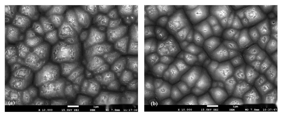
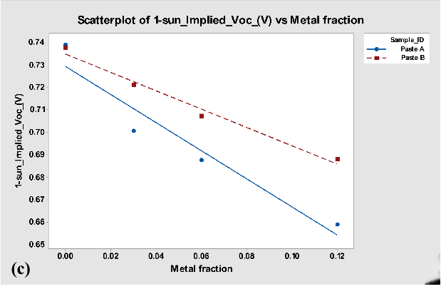
Figure 1: (a) Sample after silver paste A was used to remove the silver and glass layers (b) Sample after silver paste B was used to remove the silver and glass layers (c) Voc values of silver paste A and silver paste B corresponding to different metallization areas.
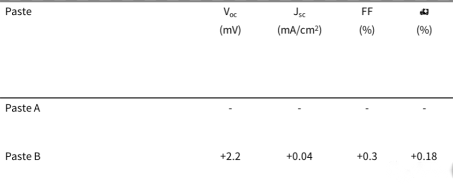
In addition, silver paste A and silver paste B were tested on full-scale production line n-type PSPC silicon wafers with 150nm n+ polysilicon layers. The scanning electron microscopy showed that the less etched silver paste B produced a cell with a Voc gain of 2.2mV and a filler factor gain of 0.3%, resulting in an absolute efficiency improvement of 0.18% (see Table 1).
Comparison of the efficiency of slurry on TOPCon solar cells with thick 160nm polysilicon layers in the production line
2 New inorganic system suitable for low-temperature sintering
Polysilicon layer thinning brings two benefits to cells:
1. Increase the production volume of the deposition process, thereby reducing the cost;
2. Reduce the parasitic light absorption of the polysilicon layer, thereby improving the light utilization efficiency.
To maintain the quality of thin thickness polysilicon layers, silicon wafers are best sintered at lower temperatures. The physicochemical properties of glass play a decisive role in the optimal sintering temperature or the range of the silver paste sintering window. For the thin polysilicon layer structure, the researchers specially developed a special glass system whose contact resistivity can be consistent in a sintering window wide of 50⁰C, and the overall efficiency is improved at lower temperatures.
As shown in Figure 2, where silver paste C is the reference sample and silver paste D contains specially developed glass, the efficiency of silver paste C decreases with a decrease in peak firing temperature due to a severe decrease in FF. Conversely, the Voc, FF, and efficiency of silver paste D increase, while the peak sintering temperature decreases. Silver paste D at 50°C below standard temperature has an efficiency gain of 0.2% over reference sample slurry C at standard sintering temperature.
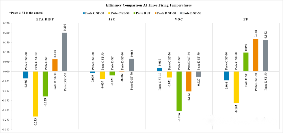
Figure 2: Relative values of silver pastes C and D sintered below the standard peak temperature of 30°C (ST-30), 50°C (ST-50) and standard peak temperature (ST).
As shown in Figure 3, the contact resistivity of silver paste C increases significantly with the decrease of firing temperature, while the contact resistivity of silver paste D at three firing temperatures is very stable in the range of 1.1-1.7 mohm·cm2.
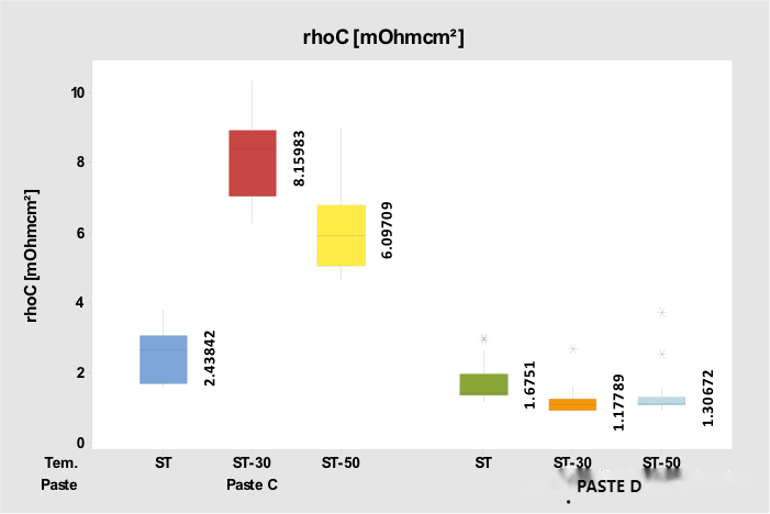
Figure 3: Contact resistivity (Rhoc) of silver paste C and D sintered below standard peak temperature 30°C (ST-30), 50°C (ST-50) and standard peak temperature (ST)
In addition, for the back TOPCon structure in addition to SiNx, polysilicon layer and tunneling oxide passivation layer, there is AlOx passivation layer, a new inorganic system was developed, which can still form good contact at low temperature (ST-50), while maintaining the passivation effect to the greatest extent, Figure 4 shows the special inorganic design slurry F compared to the reference slurry E sintered EL photo, it can be seen that in the case that the normal slurry cannot contact EL blackening, F slurry EL bright. Good contact is formed.
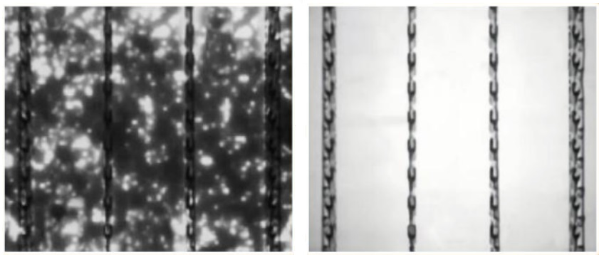
Figure 4: (a) EL photo after low temperature sintering of E slurry (b) EL photo after low temperature sintering of F slurry
In order to match the low-temperature sintered N-type TOPCon backside slurry, a front-side boro-expanded silicon wafer contact slurry has also been developed to minimize the composite caused by metallization, while maintaining high contact with different square resistances and different suede silicon wafers, and the new organic system will be compatible with finer grid line printing, so that the overall efficiency of the cell is optimized and improved.