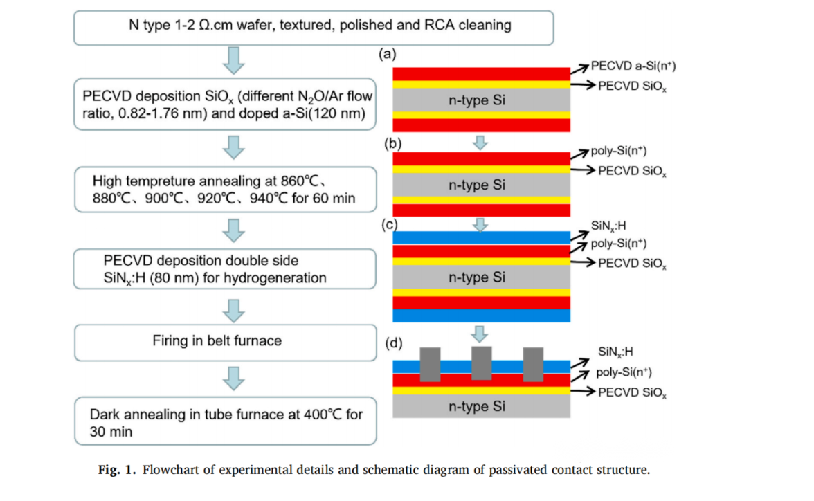
PE-Poly tunneling oxide film formation
Jan 02, 2024
Key conclusion
- The tunnel oxide layer prepared by PE method has an optimal film thickness, and the film quality of the tunnel layer is directly related to the concentration of O atoms excited by plasma
- The degree of internal expansion of n-poly Si has an optimal range for passivation and contact properties
- The higher the annealing temperature is, the higher the activation P concentration is, and the synchronous expansion will increase
Experimental scheme
- Silicon wafer: N-type silicon wafer, resistivity 1-2 Ω·cm, after milling → polishing →RCA cleaning silicon wafer
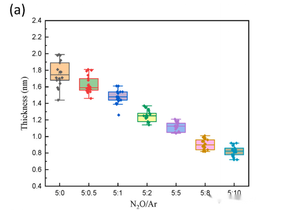
- Tunneling oxide deposition variable: N2O/Ar different flow ratio (5/0→5/10), film thickness 0.82-1.76nm
- Amorphous silicon a-Si thickness 120nm: SiH4/Ar/PH3=1/5/1
- High temperature annealing: time 60min, temperature 860-940℃
- PECVD double-side coating SiNx:H, double-side passivation
- Sintering furnace fast burning
- Tubular dark annealing 400℃
Measurer
-
- Four-point probe
- In situ OES spectrometer was used to detect O content
- sinton WCT120: Measure iVoc, Jo
- Factors examined by TLM
- Membrane formation rate and uniformity of tunneling layer
- Effect of annealing on internal expansion
- Passivation property
- Contact resistivity
Result discussion
N2O/Ar PE tunneling oxide film formation rule
- With the increase of the proportion of Ar flow, the film formation rate of the tunnel oxide layer decreases, the film thickness convergence is narrow, and the uniformity is improved (the range is from 0.55 nm to 0.17 nm).
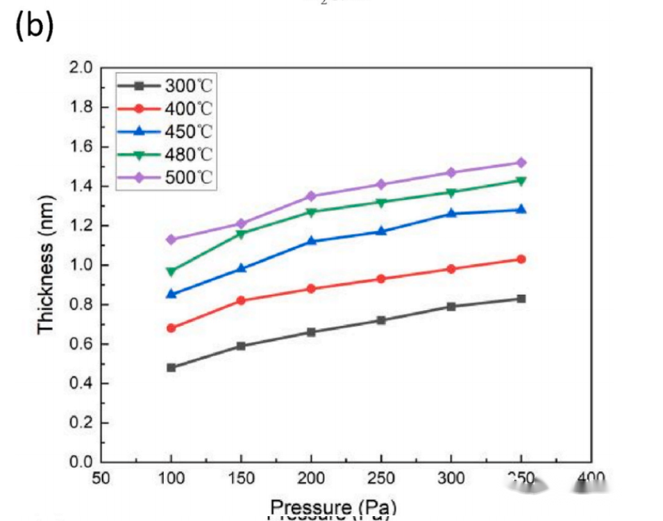
- In the range of 100Pa-300Pa, the thickness of oxide layer increases with the increase of deposition pressure
- In the range of 300-500℃, the thickness of oxide film increases with the increase of deposition temperature
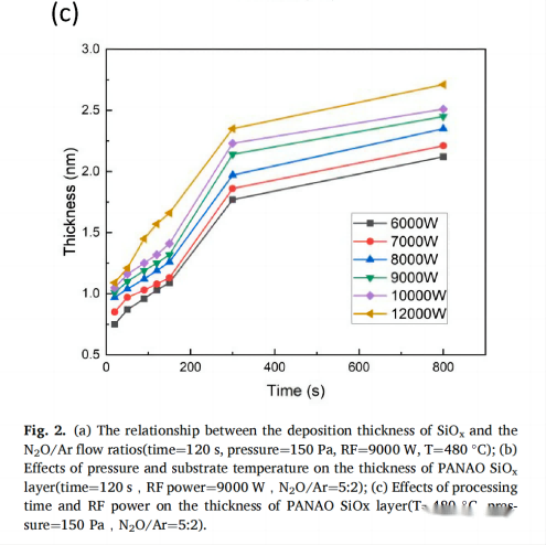
- The film formation rate of the tunnel oxide layer is the highest in the first few tens of seconds, and then the deposition rate gradually decreases
- In the range of 6-12KW, the higher the RF power, the faster the deposition rate
OES pattern
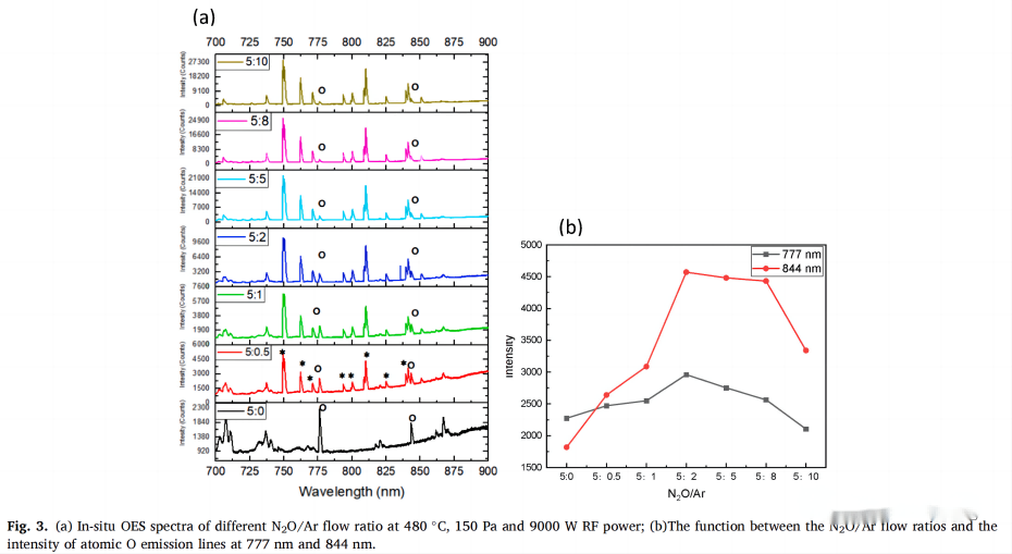
- O atomic emission spectra peak corresponding to 777nm(3P⁵→3S⁵ conversion), 844nm(3P⁵P→3S⁵S conversion)
- When the N2O/Ar flow ratio is 5/2, the emission line of O atom reaches the maximum value
Doping curve effect
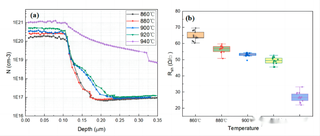
- The annealing temperature is 920℃, and the doping amount is activated5×10²⁰cm⁻³
- The corresponding peak doping concentration of different groups is the same
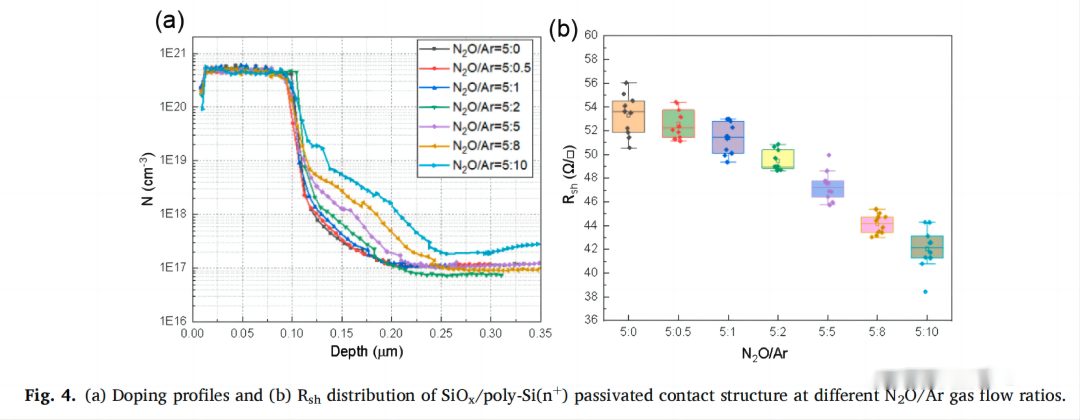
- The P doping amount of internal expansion into silicon body, the thicker the oxide layer is, the less the internal expansion is. The denser the oxide layer, the less internal expansion
- With the decrease of oxide film thickness, the internal expansion increases and the back square resistance decreases
- The introduction of Ar can improve the square resistance uniformity, and the best N2O/Ar flow ratio is 5/2
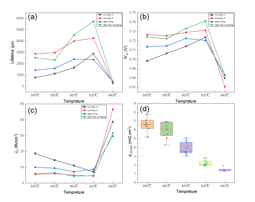
Annealing temperature effect
- The annealing temperature is 860→940℃, and the resistance decreases with the increase of temperature. When the annealing temperature reaches 940℃, the plunge value of square resistance is 26Ω/sq, which corresponds to the serious internal expansion of doping curve.
- The P concentration of peak activation increases with the increase of annealing temperature
Passivation capacity
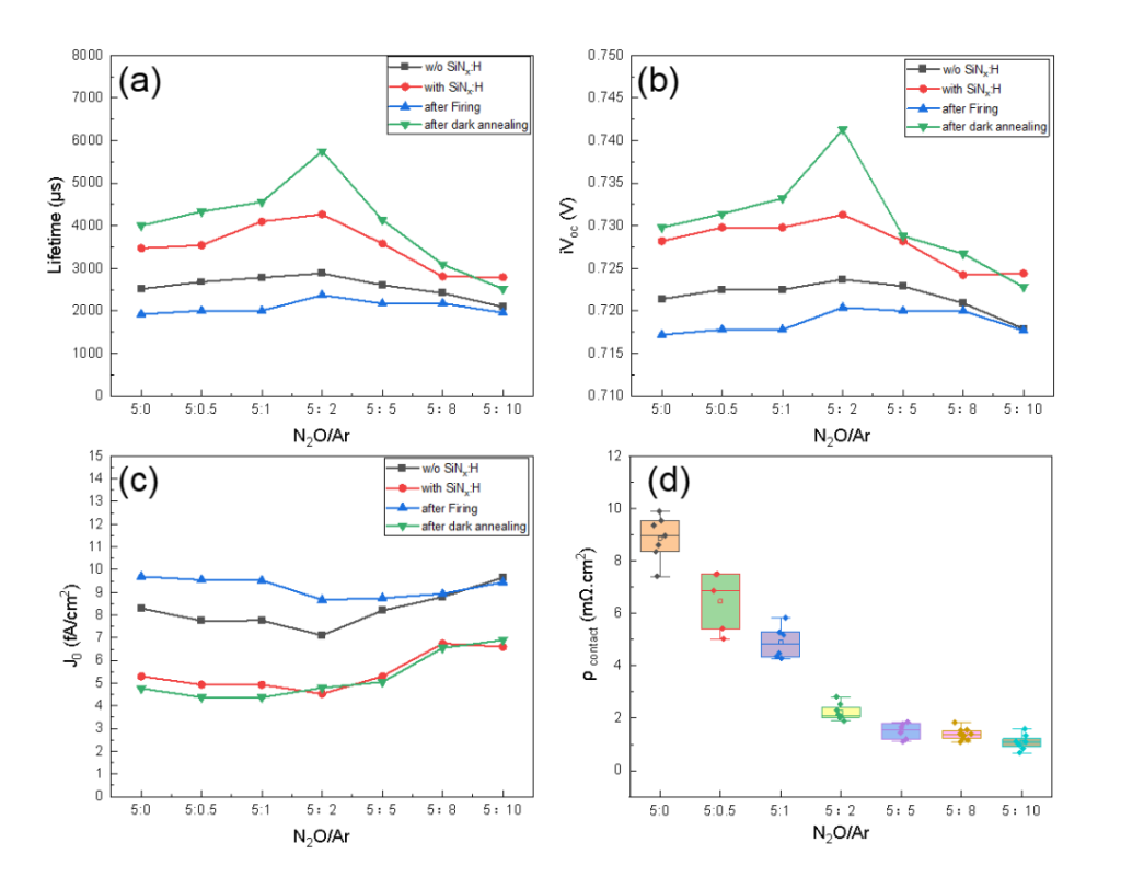
- The passivation effect of the optimal group is iVoc 741mV Jo4.8fA /cm2
- At the same time the contact resistivity is low


 English
 español
 한국의
한국의


 IPv6 network supported