

One of the major optical losses in solar cells is surface light reflection. The surface light reflection loss of polished silicon wafers is up to 34%, and the reflection must be reduced to ~10% or less in order to prepare high-efficiency solar cells. In crystalline solar cells, suede is often made on the surface of the silicon wafer, and the surface light reflection of the suede is reduced, which means that more light enters the solar cell, thus producing more photogenerated carriers. At the same time, the effective suede structure makes the incident light reflect and refract on the surface for many times, which changes the direction of the incident light in the silicon, prolongs the optical path, and produces light trapping, thereby increasing the generation of photogenerated carriers.
 Schematic diagram of the light trapping of the suede of a silicon wafer

Pyramid 3D drawing
At present, the texturing process mainly includes:
1. Etching of the damaged layer of silicon wafer
The slicing process will cause cutting damage and residual impurities on the surface of the silicon wafer, and the damaged layer and residual impurities will not be conducive to the improvement of cell performance. The figure below shows the surface topography of monocrystalline silicon wafers. Therefore, it is necessary to treat and inspect the surface of the silicon wafer before proceeding to the cell manufacturing process to ensure the elimination of damaged layers and residual impurities. A common process for etching purposes is lye etching, and the most commonly used etching solution is NaOH, KOH or TMAH (tetramethylammonium hydroxide) solutions. Due to the different energies of silicon atoms in different crystal planes, the alkali etching process shows anisotropy, but the degree of anisotropy can be changed by adjusting the etching conditions.
After the etching of the damaged layer is completed, the silicon wafer must be cleaned and inspected, and there can be no residue, which will affect the quality of the subsequent texturing process.
 Diamond wire-cut monocrystalline silicon wafer (cutting marks are clearly visible)
2. Alkali texturing
About 95% of solar cells in the PV industry are manufactured from monocrystalline and polycrystalline silicon wafers. Silicon crystal is a diamond lattice structure, and {100} monocrystalline silicon wafers are commonly used in production, because it is relatively easy to alkali texturing. Alkali texturing refers to the etching of silicon with alkali solution, forming a structure on its surface to reduce light reflection, resulting in anisotropic etching, and preparing a pyramid structure on the surface of the silicon wafer, as shown in the figure below. The biggest difference between texturing and damage layer etching is the degree of etching, in order to enhance the anisotropy characteristics of lye etching, the etching speed of the texturing process must be low, such as 2μm/min or less.
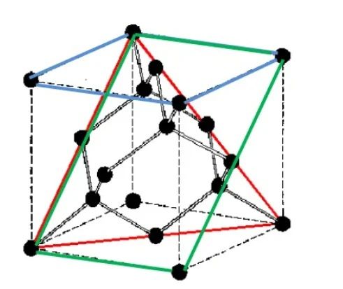
Silvaria diamond lattice structure
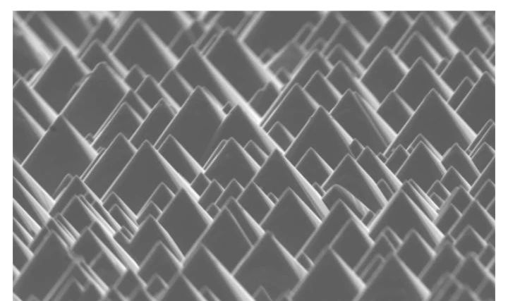
A pyramidal structure randomly distributed on the surface of a silicon wafer
The main factors affecting the quality of alkali texturing process are as follows:
a. Silicon surface quality before texturing: The silicon surface residue or defects in the texturing process are sensitive, and it needs to be tested before the texturing process to ensure that the surface of the silicon wafer is absolutely clean.
b. Etching time: There is pyramid formation and corrosion in the etching process, and the pyramid shape will be destroyed if the etching time is too long.
c. Etch solution concentration and reaction bath temperature: As shown above, anisotropic etching requires controlling the etch concentration and temperature.
d. Concentration of IPA: IPA can continuously evaporate from the reaction solution, affecting the etching process.
3. Acid texturing
Acid texturing is the roughening of the surface of polycrystalline silicon silicon wafers to reduce the reflection of light. Polysilicon is composed of grains of different orientations, making it unsuitable for anisotropic etching with alkaline solutions. This is because the etching speed varies in different directions, resulting in non-uniform variations in silicon thickness. In addition, there are a large number of grain boundaries in polycrystalline silicon wafers, and the etching at the grain boundaries when using lye etching will cause dislocations and affect cell performance.


 English
 español
 한국의
한국의


 IPv6 network supported