

1. LECO Laser assisted sintering technology
Laser assisted sintering technology is also known as laser enhanced contact optimization,Patented in 2016 by Cell Engineering GmbH for repairing undersintered PERC cells, LECO is an advanced laser sintering technology for improving the contact between metal electrodes and silicon wafers in solar cells.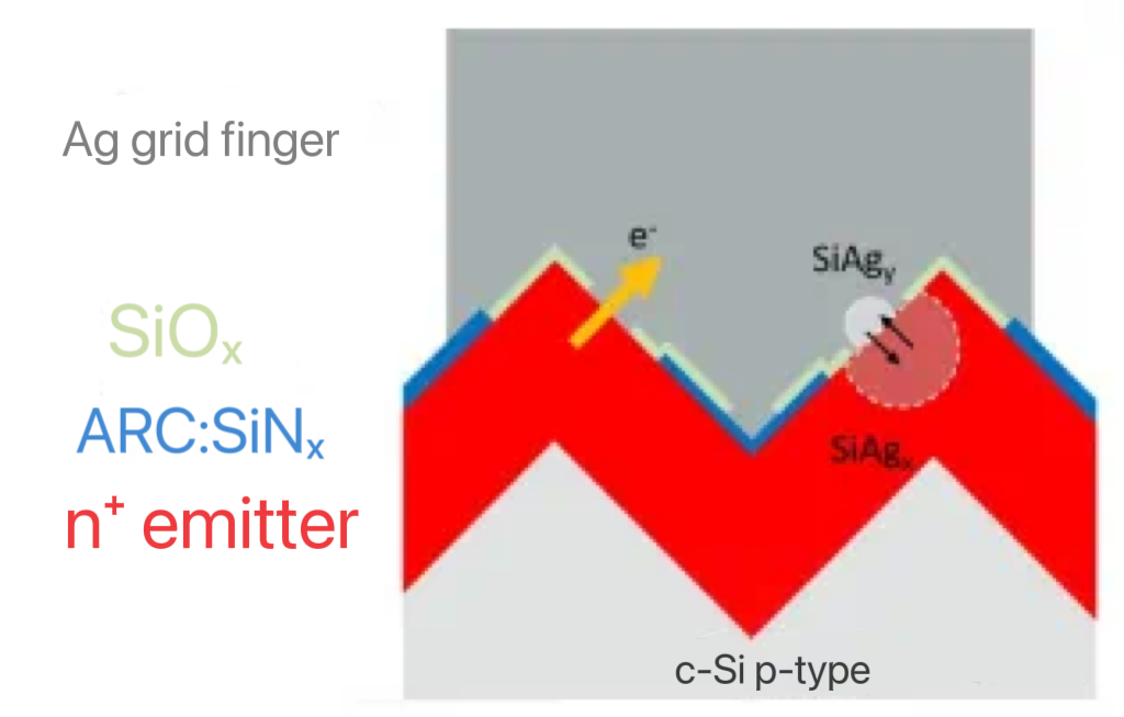
2. LECO laser assisted sintering principle
The technology uses a high-intensity laser to illuminate the battery to stimulate charge carriers, while applying a deflection voltage of 10V or more, resulting in a local current of several amps, and the corresponding sintering triggers the mutual diffusion of silver paste and silicon, which will significantly reduce the contact resistance between the metal and the semiconductor. Laser-assisted sintering allows for a larger sintering temperature window, correct contact at ultra-low doping emitters, and allows for higher voltage VOCs, making laser-assisted sintering more competitive than standard sintering.
3.LECO laser assisted sintering
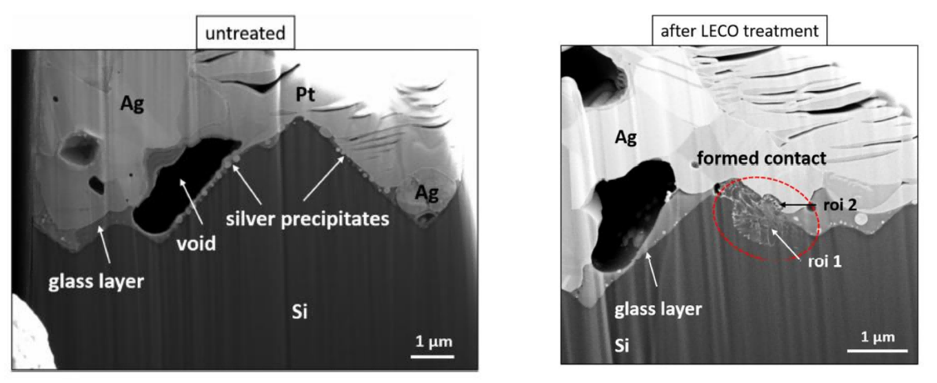
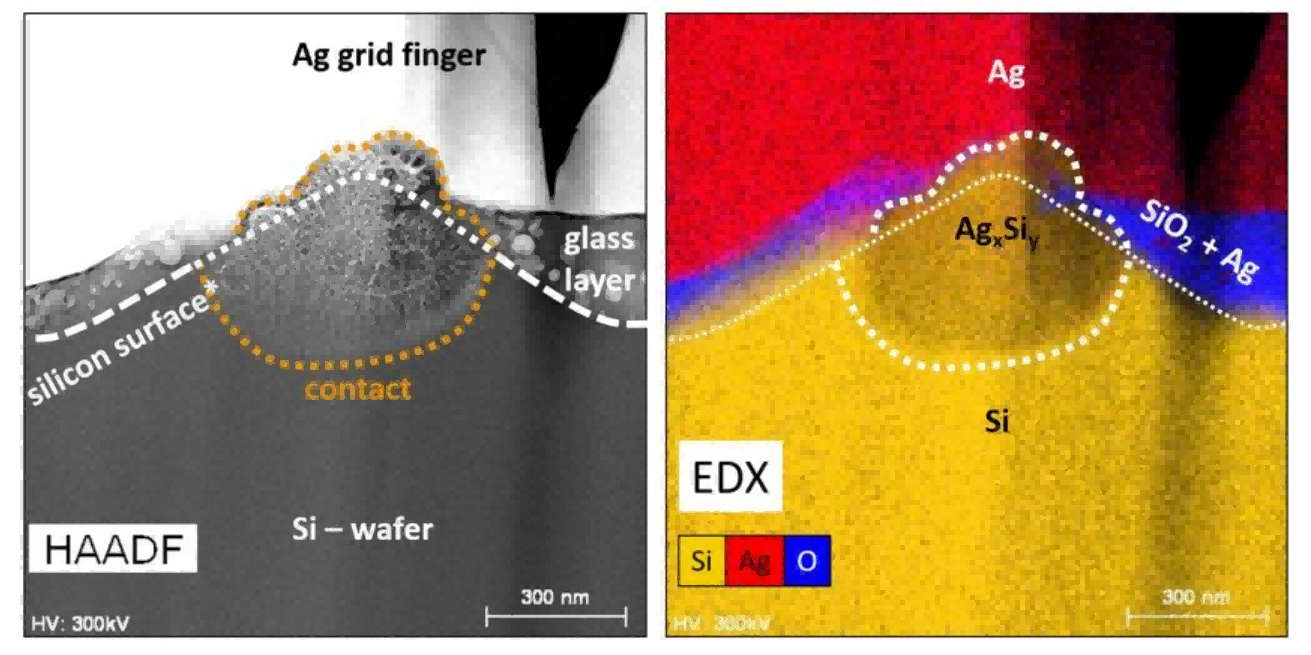
SEM images of contact interface before and after LECO treatment
Mainly because the laser can accurately heat the silver paste, locally destroy the passivation layer, so that silver can directly form contact with silicon, under the premise of not damaging the silicon wafer, to promote the silver paste local melting and diffusion into the surface of the silicon wafer, forming a tiny silver silicon alloy junction, which has a very low contact resistance, and the transmission efficiency of electrons is very high.
4. LECO laser assisted sintering advantages and disadvantages
advantage
① LECO can improve the conversion efficiency of solar cells by optimizing metal contact and reducing contact resistance, so that higher currents can be obtained under the same linewidth, or thinner lines can be obtained under the same current.
② The laser process allows very precise control of the heat-affected zone, which allows the passivation layer to be destroyed and metal contact formed without damaging the active zone of the battery.
③ The traditional hot sintering process may cause damage to the whole silicon, LECO as a non-contact technology, the risk is lower, and the thermal stress and damage to the silicon wafer are reduced; Fourth, the LECO process has a high degree of automation and can be integrated into high-speed production lines, which helps to improve the consistency and reliability of battery production.
④ Because laser processing can be very precise, it can reduce the amount of metal used and reduce manufacturing costs. In addition, LECO is suitable for rich integration levels and a wide range of battery types.
⑤ The use of LECO technology can avoid the complex doping process of LSE technology and the use of laser equipment, the production line is simpler and faster, while reducing manufacturing costs, but also reduce potential sources of manufacturing error.
shortcoming
① LECO equipment requires an initial investment.
② Special silver paste is also more expensive than traditional silver paste;
③ Laser sintering is a complex process that requires accurate laser parameter control and process management;
④ High-precision laser equipment requires professional maintenance and operation, which may increase labor costs and equipment maintenance costs.
⑤ The operation of laser equipment needs to strictly comply with safety procedures to prevent harm to the operator or the environment.
difficulty
① The difficulty of LECO technology lies in process optimization and material compatibility. First, in terms of process optimization, finding the best laser parameters (such as power, duration, and focus size) to maximize efficiency gains while minimizing wafer damage is a challenge.
② The development and selection of silver paste materials compatible with the laser process to ensure good contact formation and stability during the sintering process is also a difficulty.
5.LECO laser assisted sintering efficiency
TOPCon solar cells using LECO technology can improve their conversion efficiency, typically between 0.2% and 0.5%.
6. LECO laser assisted sintering process
LECO's process is to shine a high-intensity laser on the battery while applying a deflection voltage of 10V or more, resulting in a local current of several amps that significantly reduces the contact resistance between the metal and the semiconductor. Under experimental conditions, the processing time per wafer is 1.6 seconds, which can be easily reduced to less than 1 second.
The specific process flow is as follows:
① Preparation: First of all, the silicon cell is deposited with the passivation layer through the conventional process steps to form a high-quality passivation layer to reduce surface composite.
② Silver paste printing: The silver paste is coated on the front surface of the silicon wafer using screen printing or other printing technology to form a predetermined electrode pattern. Silver pulp contains silver particles as well as organic solvents and adhesives.
③ Pre-drying: Before laser treatment, the silicon wafer coated with silver paste is pre-dried to remove most of the organic solvent, so as to avoid the gas bubbles generated by laser heating affecting the contact quality.
④Laser sintering: By precisely controlling the energy and irradiation time of the laser, the laser is irradiated on the silver paste, and the silver paste is locally heated for sintering. The thermal effect of laser leads to the melting and joining of silver particles in the silver paste.
Expansion: Microscopic changes between the silver paste and the cell during this process
① Local destruction of passivation layer: Hot spots caused by laser heating will locally destroy the passivation layer on the silicon chip, which is a precisely controlled physical process. The passivation layer is destroyed to enable the silver to form direct contact with the silicon wafer, establishing an efficient electron transport path.
② silver-silicon alloy formation: Under the action of high temperature, silver particles begin to react with silicon to locally form silver-silicon alloy. This process involves silver atoms diffusing into the surface of the silicon wafer and forming a good ohmic contact in the contact area.
③ Cooling and curing: After laser treatment, the sintering area begins to cool. The metal connection between the silver particles solidifies to form a strong electrode.
④ Cleaning and inspection: Finally, the treated silicon wafer is cleaned to remove any residual organic matter, and inspected to ensure contact quality and battery function.


 English
 español
 한국의
한국의


 IPv6 network supported