

Knowledge
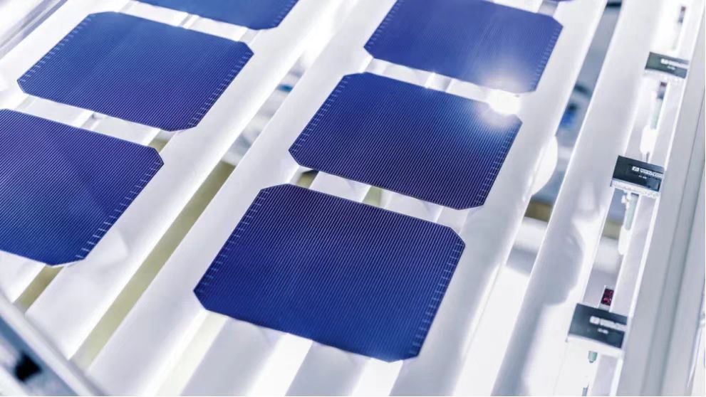
Double-sided passivated emitters and backside cells (PERCs) currently have the highest share of the PV market. However, heterojunction (HJT) and tunnel oxide passivation contact (TOPCon) solar cells are expected to gain significant market share soon. Despite technological advances, concerns about th...
Read More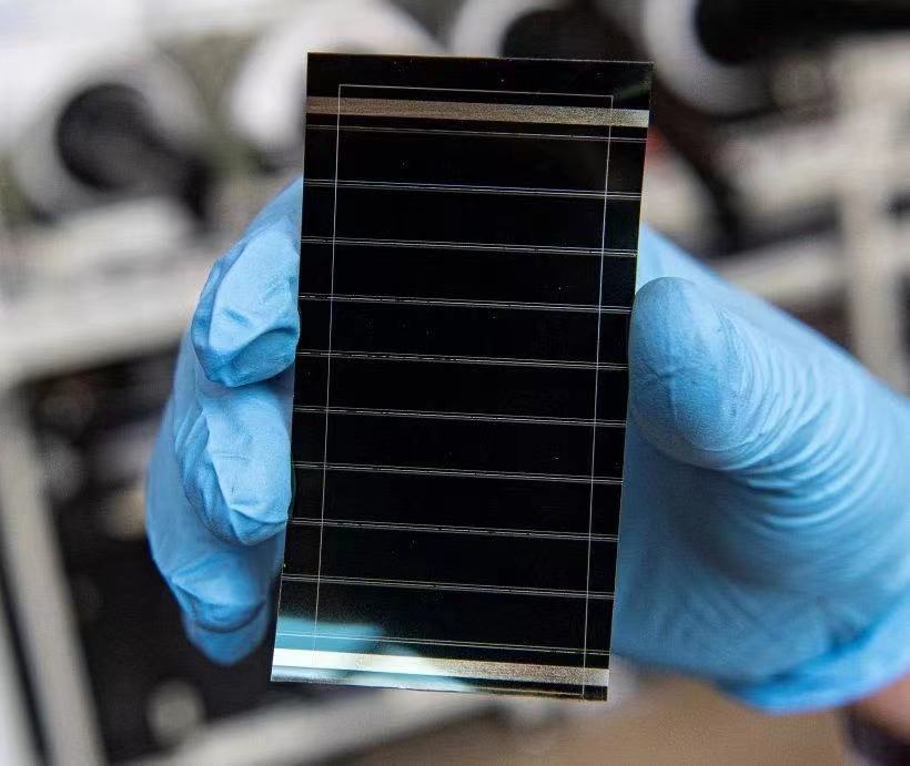
Researchers at the University of North Carolina at Chapel Hill and Arizona State University designed a large-area perovskite-silicon tandem solar cell with an open area of 24 square centimeters and achieved a steady-state efficiency output of 25.1%. Current-voltage curve of a perovskite micromodule...
Read More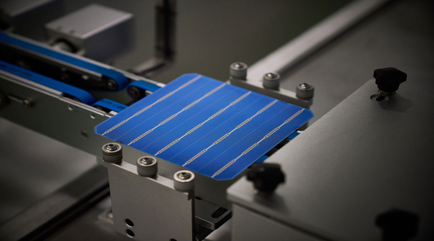
1. XBC solar cell technology (1) BC is not a completely new solar cell technology Back Contact, metal electrodes are arranged on the back of the solar cell in a cross-finger shape, creating more light-absorbing area for the front and improving the overall photoelectric conversion effic...
Read More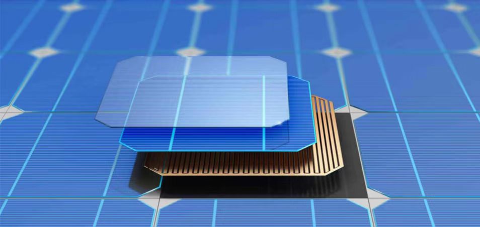
First, copper electroplating helps reduce costs and increase efficiency in the metallization of photovoltaic solar cells 1.1 Constrained by high-cost silver paste, the metallization process of photovoltaic cells needs to be innovated urgently Photovoltaic solar cells are the most core devices for ph...
Read More
The efficiency of N-type polysilicon backside passivated contact (PSPC) cells manufactured on industrial production lines has increased from 20.7% to 23.6% or higher in the past three years. The rapid efficiency climb is strongly supported by metallized pastes that can contact both the boron emitter...
Read More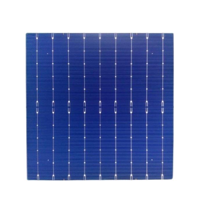
Frontal metallization: efficiency accelerator n-TOPCon SE creates more room for efficiency Compared with the conventional p+ emitter, the p+ emitter SE process has a shallower junction in the non-metallized region, a deeper junction in the metallized region, and the surface concentrati...
Read More
In the past three to five years, the photovoltaic industry's solar cell technology has been rapidly upgraded and iterated, and high-efficiency PERC solar cells have gradually replaced traditional all-aluminum back-field solar cells and become a new generation of "conventional" solar cells. So, after...
Read More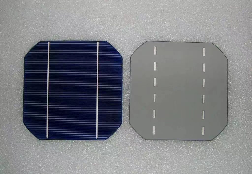
What is photovoltaic silver paste? The main principle of photovoltaic power generation is the photovoltaic effect of semiconductors, that is, when the silicon wafer is illuminated, the charge distribution state in the body changes to generate electromotive force, converting photons int...
Read More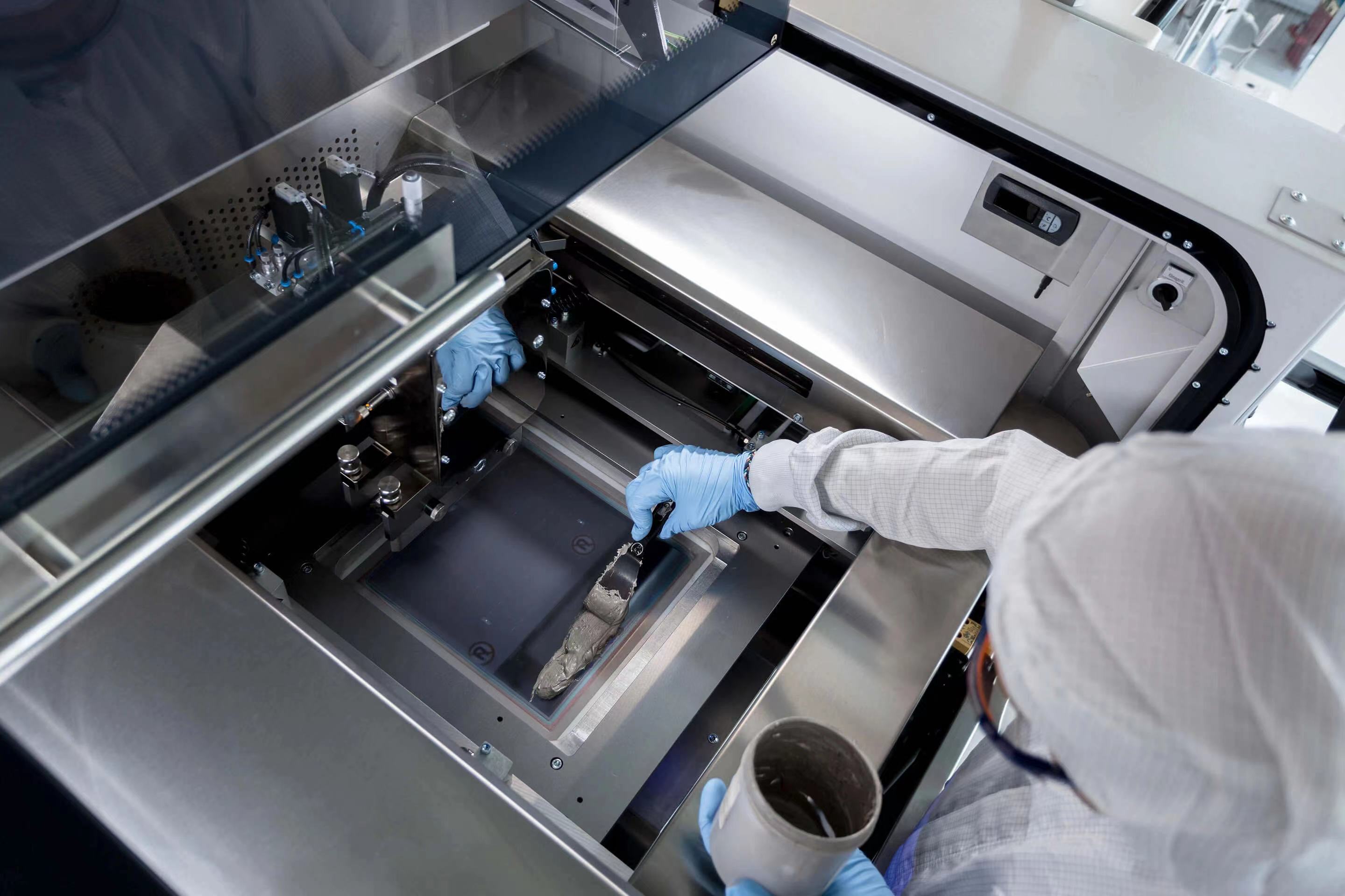
In the manufacturing process of solar cells, in order to prepare solar cell contact electrodes, it is necessary to print metal paste on silicon wafers using screen printing technology. After the sintering process, front and back electrodes are formed on the surface of the solar cell thr...
Read More
Laser-enhanced contact optimization (LECO), or laser-enhanced contact optimization, patented by Cell Engineering GmbH in 2016, replacing the conveyor furnace (FFO) technology typically used for TOPCon solar cell. In principle, the current formed by the laser is transmitted along the p...
Read More
After purposeful doping, the semiconductor bulk silicon introduces trace impurities to become an extrinsic semiconductor, which is divided into N-type and P-type two categories. 1. N-type crystalline silicon When the crystal silicon is mixed with trace impurities Group V elements, its five valence e...
Read More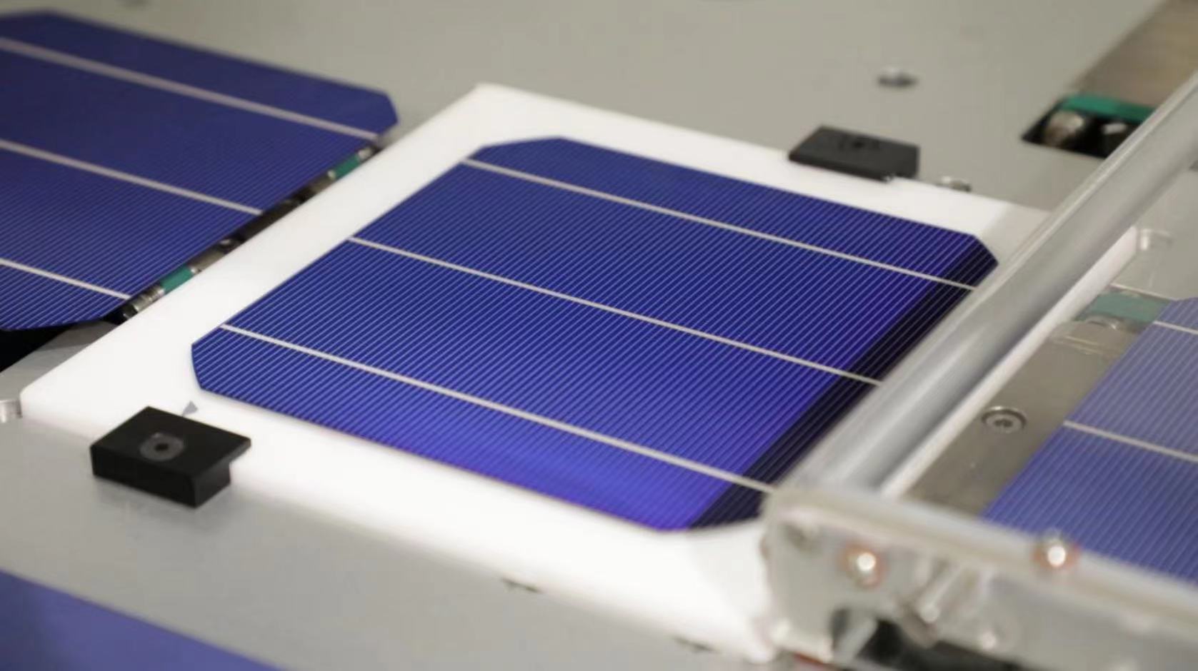
The manufacture of crystalline silicon modules involves fabricating silicon wafers, transforming the wafers into cells, and assembling cells into modules. A wafer is a thin, flat disk or rectangle of base semiconductor material. Wafers are 180μm to 350μm th...
Read More


 English
 español
 한국의
한국의


 IPv6 network supported