

Knowledge
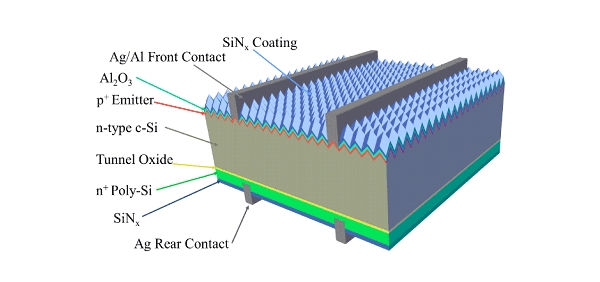
Atomic layer deposition (ALD) technology is widely used in micro-nano electronics, energy storage and other fields due to its excellent controllability, uniformity and conformality. Under the conditions of 200°C and 60 rpm, trimethylaluminum and water were used as precursors to form high-quality...
Read More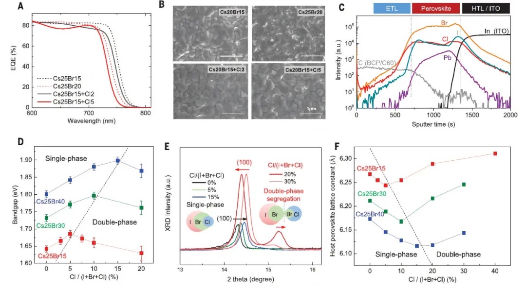
Wide bandgap metal halide perovskites are ideal semiconductors for use in combination with silicon stacks to achieve power conversion efficiencies (PCE) exceeding 30% while reducing costs. However, wide bandgap perovskite solar cells are fundamentally limited by light-induced pha...
Read More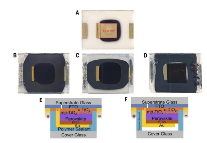
The energy conversion efficiency of perovskite solar cells (PSCs) has increased from 3.8% to 25.2% and beyond in 10 years, but their commercialization is limited by instability. Researchers have developed a low-cost polymer/glass tandem packaging solution that enables PSCs to pas...
Read More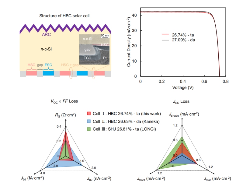
The development of BC cells has reduced the cost of photovoltaic power generation, but the diversification of application scenarios has put forward higher requirements for solar cell technology. Studies have found that the contact resistivity of HBC solar cells has a great influence on cell per...
Read More
Solar energy has attracted attention as a future energy source. Among the several BC cells (HPBC, TBC, HBC) for next-generation products, HPBC is a direction for the development of solar cell technology. HPBC cells combine the advantages of passivated emitter and back surface pas...
Read More
The percentage of PV module output power to the total power of the cell (CTM) is an important parameter to measure the degree of power loss in module packaging. The promotion and application of high-efficiency cells such as PERC, TOPCon, HJT and XBC cells have made new packaging...
Read More
The solar photovoltaic industry is seeking to improve module performance through innovative manufacturing processes, new materials, solar cell designs and module configurations. SHJ solar cells have advantages such as high PCE, simplified manufacturing processes and low manufacturing tempe...
Read More
As the mainstream solar energy core conversion technology in the market today, the performance optimization of crystalline silicon solar cells depends on the precise design of the structure and the monitoring of the manufacturing process, among which the PN junction doping contro...
Read More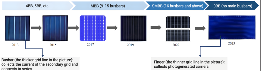
Cost is an important factor restricting the industrial development of high-efficiency N-type solar cells. Among them, the cost of metallization silver paste accounts for the highest proportion of the cost except for silicon materials. With the development of the next generation of n-type high-effici...
Read More
The screen used in the screen printing process is a key consumable in the photovoltaic industry. It is mainly used for electrode formation and conductivity improvement. The paste (such as silver, aluminum, etc.) is accurately pressed on the silicon wafer through screen printing to form an elect...
Read More
Solar energy as the future energy is concerned, in the next generation of products of several BC cells(HPBC, TBC, HBC), HPBC is a direction of the development of solar cell technology. HPBC cell combine the benefits of passivated emitter and back surface passivated contact technology (PERC) and adop...
Read More
Tandem solar cells are a type of solar cell that combines two or more different photovoltaic materials in a single device. This allows tandem cells to capture a wider range of the solar spectrum and generate more electricity than single-junction cells. One promising combination for tandem solar cell...
Read More


 English
 español
 한국의
한국의


 IPv6 network supported