


Issue
Effect of B expansion doping curve on n-TOPCon cell
1.I-V parameters: VOC/FF/RSER/JSC
2.Peak concentration
3.Junction depth
4.Saturation current density 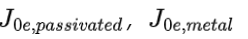
5.Contact resistivity 
Key conclusions
1.Saturation dark current effect
With the increase of junction depth and peak concentration, the passivation zone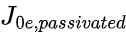 becomes larger. The reason is the intensification of surface recombination and bulk recombination
Reduce the saturation current density in the passivation zone in the direction of low surface concentration + shallow junction
In the range of 0.5~0.85 μm junction depth, the peak concentration increases with the increase of junction depth, and the gold semi-contact area  becomes smaller. It can be explained by the concept of "transmission-limited emitter" (insensitive to bulk recombination): the hole concentration in the heavy doping region of the emission region is very high, the hole lifetime is low, and therefore the hole recombination rate is also low. Increasing the doping concentration can reduce the saturated dark current density in the gold half-contact region. When the junction depth is greater than 1.0 μm, the saturation current density in the gold semi-contact region increases, which is mainly due to the aggravation of bulk recombination.
Reducing the saturation dark current in the gold half-contact region can increase the heavy doping area, increase the doping concentration and the appropriate junction depth ~0.8um
SE technology combines the advantages of light expansion area (passivation area) and heavy expansion area (gold semi-contact area).
The corrosion depth of Ag/Al slurry is 0.45~0.63 μm, which is more than 5 times higher than the width of the depletion zone
When the B doping concentration is greater than the above, the recombination of the gold half-contact region will be significantly increased. The results show that the critical point of B-doping concentration at a depth of 0.63 μm is lower than that of E+18
2. Contact resistivity
As the peak doping concentration increases, the junction depth increases and the contact resistivity decreases
With the same junction depth, the contact resistivity can be reduced from 4.5 to 1.1 mΩ/cm2 by increasing the doping concentration
The doping peak concentration is constant, and the contact resistivity can be reduced to 1.1 mΩ/cm2 by increasing the junction depth
3. iVoc impact
QSSPC method, the value is 1E15 cm-3 excess carrier concentration, and the iVoc value is 1-sun under light conditions
The junction depth is the same, and the iVoc decreases as the peak concentration increases
The peak doping concentration was the same, and the iVoc decreased as the junction depth increased
Compared with the peak doping concentration, the junction depth has a greater effect on iVoc, and the iVoc can reach 710+ mV by double-sided boron expansion + AlOx/SiNx passivation of the suede sheet
Discuss
It is reported in the literature that the lowest composite current density of n+ poly-Si emitter:
1.Under passivation , ~ 1.4 fA/cm2, polished sheet
2.Gold semi-contact region, ~ 35 fA/cm2
3.B-doped p+ layer emission zone recombination:
4.Non-gold half-contact zone: can be reduced to 11 fA/cm2 150Ω/sqr
5.The Ag-Al gate contact zone is as high as 1000 fA/cm2 before optimization and can be as high as ~300 fA/cm2 after optimization
Preparation method of doped emitter:
1.BBr3/BCl3 tubular diffusion
2.Boric acid diffusion
3.B ion implantation
Goal: Reduce the dark current density of emitter saturation and increase iVoc. How it works:
1.Front surface B expanded emitter p+ layer, low surface concentration + shallow junction
2.The resistivity of gold half-contact should be low enough to ensure contact performance
3.How to optimize the characteristics of Ag/Al slurry and the high composite of gold half-contact area?
Deep junction doping reduces the recombination loss in the gold half-contact region
High surface concentration – > low contact resistivity
Summary of previous literature:
The Al2O3 dielectric film has a fixed negative charge and has a good passivation effect on the B-expanded emitter
After wet chemical treatment, the SE method can increase the Jsc ~0.3 mA/cm2
APCVD SE, Jsc increased by 0.4 mA/cm2, efficiency increased by 0.4% (abs)
After double-sided diffusion, the lifetime of silicon wafers can be increased to 1.2~1.5 ms
The addition of Te to the slurry improves the low contact resistivity and achieves a temperature range
BCl3 can be used for diffusion of B-amplified emitters
The lower peak doping concentration may increase the saturation current density and increase the contact resistivity in the gold half-contact region
Laser doping can achieve B expansion SE
ALD Al2O3/PECVD SiNx achieves good passivation effect on the B-expanded emitter
The in-situ oxidation of BBr3 during diffusion can improve the passivation effect
Replacing Ag-Al paste with aluminum-Al paste results in higher iVoc and lower grades
The thickness of the AlOx capping layer has an effect on the passivation effect of the B-ampfed emitter
The gold half-contact region under the Ag/Al gate is recombined, and the low-B doped emitter is more serious
B RVD doping
B. Diffuse emitter deep junction can effectively reduce the recombination of gold half-contact area
The thickness of BSG and the resistance of B expansion are affected by O2 flow
Propulsion temperature and oxidation temperature are the two most sensitive influencing factors for B expansion
When the doping concentration is lower than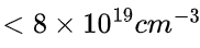 , as a current transmission mechanism, it is necessary to consider the thermal phonon emission and the thermal phonon field emission effect
The deeper the junction depth, the lower the contact resistivity
The effect of the dissipation region on the contact resistivity is negligible
Surface contamination during doping can limit efficiency
The solubility of B in SiOx is higher than that in crystalline silicon c-Si
The density of saturated dark currents after passivation of the B-spread emitter
With the increase of junction depth and peak concentration, the passivation zone becomes larger. The reason is the intensification of surface recombination and bulk recombination
Reduce the saturation current density in the passivation zone in the direction of low surface concentration + shallow junction
In the range of 0.5~0.85 μm junction depth, the peak concentration increases with the increase of junction depth, and the gold semi-contact area  becomes smaller. It can be explained by the concept of "transmission-limited emitter" (insensitive to bulk recombination): the hole concentration in the heavy doping region of the emission region is very high, the hole lifetime is low, and therefore the hole recombination rate is also low. Increasing the doping concentration can reduce the saturated dark current density in the gold half-contact region. When the junction depth is greater than 1.0 μm, the saturation current density in the gold semi-contact region increases, which is mainly due to the aggravation of bulk recombination.
Reducing the saturation dark current in the gold half-contact region can increase the heavy doping area, increase the doping concentration and the appropriate junction depth ~0.8um
SE technology combines the advantages of light expansion area (passivation area) and heavy expansion area (gold semi-contact area).

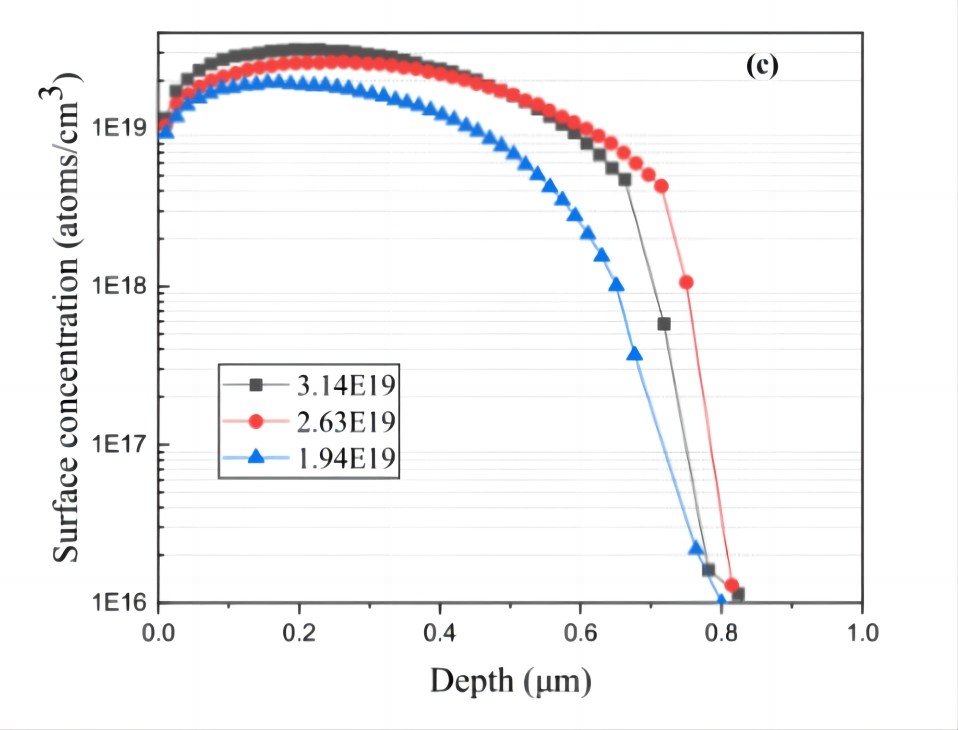 Fig. 2. ECV profiles of the change in the peak concentrations under one constant junction depth (a) Emitter D1 (d1≈0.5 μm), (b) Emitter D2 (d2≈0.63 μm), (c) Emitter D3 (d3≈0.8 μm); the change in junction depths under one constant peak concentration (d) Emitter N1(N1≈3E19 atoms/cm3 ) and (e) Emitter N2 (N2≈ 2.6E19 atoms/cm3 ).
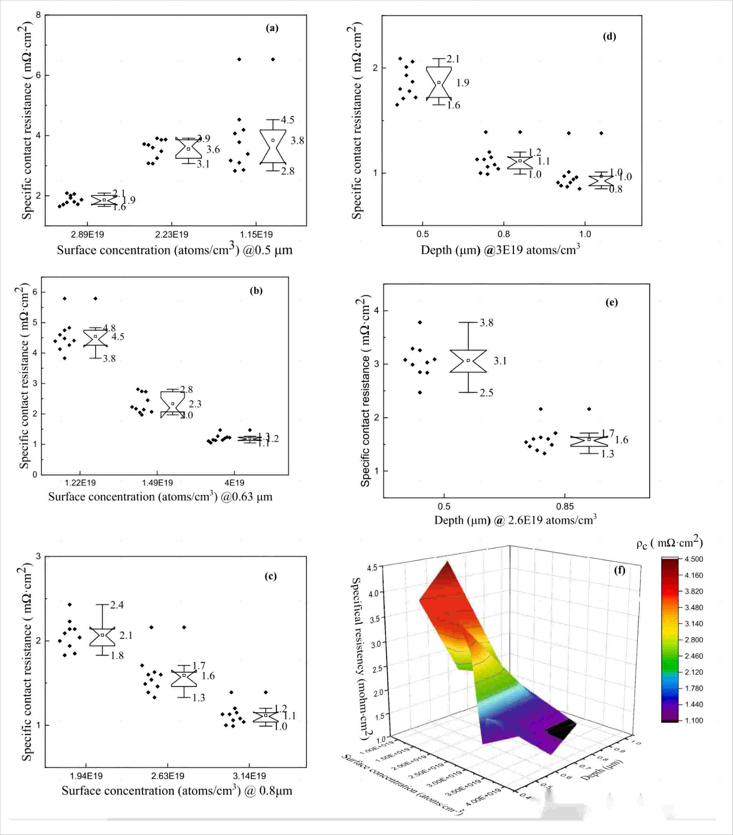
 Fig. 3. Emitter dark saturation current densities in the passivated regions of (a) emitter D1, (b) emitter D2, (c) emitter D3, (d) emitter N1 and (e) emitter N2. And (f)the J0e, passivated as a function of the junction depth and the peak concentration of B-doped profile.
 image") Fig. 4. The photograph of the screen-printing pattern of the sample with different metallization fraction from 2% to 8% (a) and Photoluminescence (PL) image (b) of the symmetrical samples were boron-diffused and passivated by Al2O3/SiNx films with our different metallization fractions on the front side. The metal was etched away before the PL measurement. The numbers in percentage indicate the metallization fractions.
Fig. 4. The photograph of the screen-printing pattern of the sample with different metallization fraction from 2% to 8% (a) and Photoluminescence (PL) image (b) of the symmetrical samples were boron-diffused and passivated by Al2O3/SiNx films with our different metallization fractions on the front side. The metal was etched away before the PL measurement. The numbers in percentage indicate the metallization fractions.
 Fig. 5. The plots of emitter dark saturation current densities in the passivation on the contact regions of (a) emitter D1, (b) emitter D2, (c) emitter D3, (d) emitter N1, (e) emitter N2 and (f) the 3D-plot of J0e, metal as a function of the junction depth and the peak concentration of B-doped profile.
Gold semi-contact interface microstructure
The corrosion depth of Ag/Al slurry is 0.45~0.63 μm, which is more than 5 times higher than the width of the depletion zone
When the B doping concentration is greater than  the above, the recombination of the gold half-contact region will be significantly increased. The results show that the critical point of B-doping concentration at a depth of 0.63 μm is lower than that of E18
 image") Fig. 6. (a) Scanning electron microscopy (SEM) image of emitter D3 sample (1.94 × 10¹⁹ atoms/cm3 ) surface after etching away the Ag–Al contact, the glass layer, the passivation layer, and all spikes. Remaining spikes imprints in red circles; (b)/(c) SEM cross section of contact spot. The shape of a corroded pyramid can be clearly seen.
Fig. 6. (a) Scanning electron microscopy (SEM) image of emitter D3 sample (1.94 × 10¹⁹ atoms/cm3 ) surface after etching away the Ag–Al contact, the glass layer, the passivation layer, and all spikes. Remaining spikes imprints in red circles; (b)/(c) SEM cross section of contact spot. The shape of a corroded pyramid can be clearly seen.
Contact resistance
As the peak doping concentration increases, the junction depth increases and the contact resistivity decreases
With the same junction depth, the contact resistivity can be reduced from 4.5 to 1.1 mΩ/cm2 by increasing the doping concentration
The doping peak concentration is constant, and the contact resistivity can be reduced to 1.1 mΩ/cm2 by increasing the junction depth
Precursor iVoc
QSSPC method, the value is 1E15 cm-3 excess carrier concentration, and the iVoc value is 1-sun under light conditions
The junction depth is the same, and the iVoc decreases as the peak concentration increases
The peak doping concentration was the same, and the iVoc decreased as the junction depth increased
Compared with the peak doping concentration, the junction depth has a greater effect on iVoc
 Fig. 8. iVoc and Lifetime of the precursor structure wafers obtained from (a) emitter D1, (b) emitter D2, (c) emitter D3, (d) emitter N1 and (e) emitter N2.
I-V parameter effects
The B doping curve can adjust for the difference between the actual Voc and the iVoc, and the difference is the effect of the busbar contact
The effect of junction depth on Voc is greater than that of peak doping concentration
Saturation current density
 Fig. S1 Measured total J0 vs. the metallization fraction f of the symmetrically the p+np+ samples for the extraction of J0 at the contact regions.
Failure analysis
Yablonovitch has a limiting current density of 46.43 mA/cm2
1. Three kinds of current loss
2. Blu-ray loss
3. Substrate collection loss
4. Loss caused by unevenness, current loss caused by uneven mass in the wafer
5. Current loss due to recombination
6. The diffusion length of the launch area and base area is insufficient
7. Affected by peak doping concentration and junction depth
8. NIR parasitic suction loss, winding plating effect
9. The deeper the knot depth, the higher the blue light loss
 Fig. 10. The curve for internal quantum efficiency (IQE) and the dashed line curve for optical reflection for (a) emitter D1, (b) emitter D2, (c) emitter D3, (d) emitter N1 and (e) emitter N2.
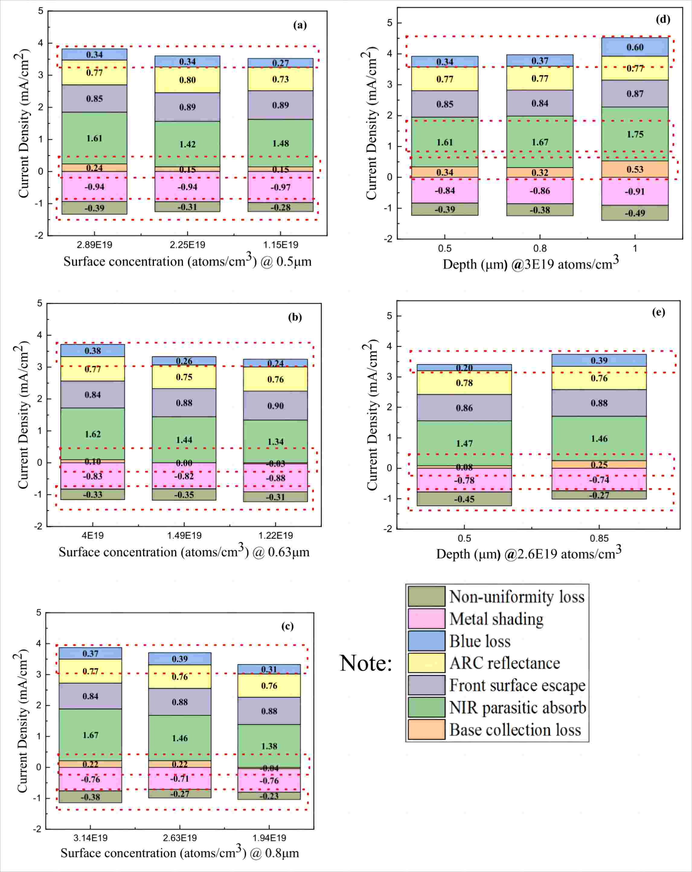
Fig. 11. Current loss mechanisms for (a) emitter D1, (b) emitter D2, (c) emitter D3, (d) emitter N1 and (e) emitter N2.


 English
 español
 한국의
한국의


 IPv6 network supported