What is a PN junction?
A PN junction is a semiconductor structure that is used as a basic component for the construction of various semiconductor devices.
How did it come to be?
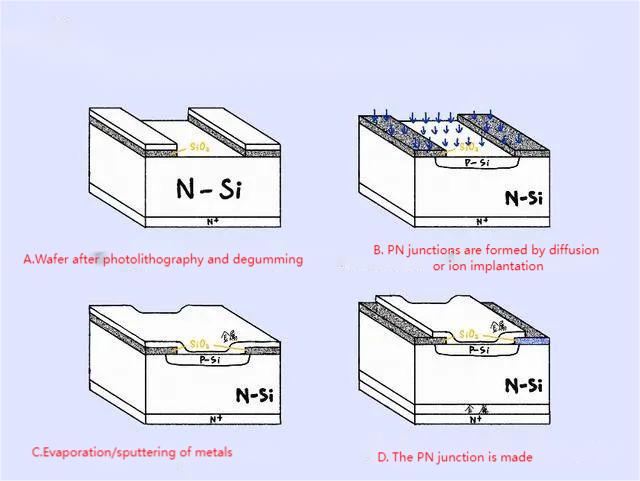
By using different doping processes to tightly bond P-type semiconductors and N-type semiconductors to form a junction with special electrical properties, intuitively speaking, P-type semiconductors and N-type semiconductors are made on the same semiconductor (usually silicon or germanium) substrate, and a space charge region will be formed at their intersection, which is called PN junction.
The main process of preparing PN junction by silicon planar process

The special electrical property of the PN junction is that it is one-way conductive, like a one-way valve, which only allows the forward current to pass through and prevents the reverse current from passing through.
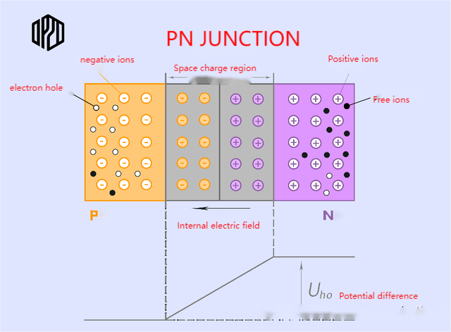
At the interface of the PN junction, diffusion motion occurs due to the difference in carrier concentrations in the P-type and N-type regions (see the previous article for an explanation of "diffusion motion"), that is, electrons move from the N-type region to the P-type region, and holes move from the P-type region to the N-type region. In this way, the P-type region will have some more negative charge and the N-type region will have some more positive charge, forming a space charge region or depletion layer. In this region, the resistance will be large due to the lack of carriers.
At the same time, in the space charge region, due to the interaction between positive and negative charges, an internal electric field is formed, the direction of which is directed from the N-type region to the P-shaped region. This internal electric field hinders the diffusion motion and causes drift motion, i.e., the carriers are moved in opposite directions by the action of the internal electric field. Eventually, in the absence of applied voltage, the diffusion motion and drift motion reach equilibrium, and the PN junction exhibits a certain built-in potential or barrier voltage.

We can use a popular metaphor to understand the formation process of PN junctions:
Suppose there are two rooms, one with a lot of balloons (holes) and the other with a lot of darts (electrons), and a door between the two rooms (interface). In the beginning, the door was closed, and the balloons and darts in both rooms were evenly distributed. We then open the door so that the balloons and darts can move freely from room to room (diffusion movement). In this way, the balloon will move from a room with more balloons to a room with fewer balloons, and the darts will move from a room with more darts to a room with fewer darts. However, during movement, the balloon and the dart collide with each other and may explode (compound).
In this way, a blank area (space charge zone) is formed near the door without balloons and darts. At the same time, in both rooms there are some post-explosion fragments (ions) that create electrostatic forces (internal electric fields) and prevent more balloons and darts from passing through the door (drift movement).
Finally, in the absence of external forces, the movement of the balloon and the dart reaches a state of equilibrium, and a pressure difference or potential energy difference (built-in electric potential or barrier voltage) is formed on both sides of the door.
If you don't particularly understand this here, especially if you are not familiar with some of these terms, it doesn't matter, let's explain them one by one.
Deplete layer
The depletion layer is another name for the space charge region in the PN junction, because in this region, most of the carriers are depleted, leaving only immobile ions.
The width of the depletion layer is usually between tens of nanometers and hundreds of nanometers and is a critical part of the PN junction. This width refers to the distance from the P region to the N region, which is often expressed by W, and depends mainly on the doping concentration and built-in potential in the P and N regions. In general, the higher the doping concentration, the narrower the depletion layer; The larger the built-in potential, the wider the depletion layer.
Built-in electric field
The built-in electric field refers to the electrostatic field generated by positive and negative ions in the space charge region of the PN junction, and its direction is directed from the N region to the P region. The built-in electric field has a hindering effect on the carriers, which weakens the diffusion motion and enhances the drift motion. The built-in electric field is also one of the reasons why PN junctions are unidirectionally conductive.
Barrier voltage
The barrier voltage refers to the potential difference between the two ends of the space charge region in the PN junction, also known as the built-in potential or contact potential. The barrier voltage reflects the difference in the energy level of the PN junction in equilibrium, which determines the energy barrier that the carriers need to overcome across the PN junction. In general, the higher the doping concentration, the smaller the barrier voltage; The higher the temperature, the smaller the barrier voltage.