

Compared to conventional solar cells, interdigitated back contact (IBC) solar cells have several special features, including back contact points and back contact, so they are not subject to the shading loss of the front metal grid. Since there is no frontal grid, the light is brighter and the series resistance is less, which improves efficiency. IBC solar cells were first discovered by Lammert and Schwartz (1977) and Swanson et al. (1984). In 2013, Fraunhofer ISE (Reichel et al., 2013) and the Inter-University Center for Microelectronics (IMEC) (Singh et al., 2014) developed an evaporative metal process to fabricate IBC solar cells with a conversion efficiency (η) of 23.0%. In 2014, the Australian National University (ANU) demonstrated an IBC solar cell with a pore size efficiency of 24.4% using passivated stacking and lithography (Franklin et al., 2016). In 2015, the Hamelin Institute of Solar Energy Research (ISFH) developed an ion implantation laser process to fabricate IBC solar cells with a η of 23.4% (Brendel et al. 2016). In 2016, SunPower announced the production of 5-inch IBC solar cells using passivated contact and screen printing technology with a η rate of 25.2% (Smith et al., 2016). Kaneka produced silicon heterojunction solar cells with a η of 26.7% interdigitated dorsal contact (HJ IBC) (Belarbi et al., 2016) (Yoshikawa et al., 2017). We have previously reported improvements η replacing traditional silver contacts and single-pass passivations by electron beam evaporation of aluminum contacts, screen printing, and stacking passivation (Chen et al., 2015, 2017). Here, we focus on micron-scale passivation contact and fit doping levels with the industrial processing of IBC solar cells.
In IBC solar cells, passivation, diffusion, and contact obviously affect the performance of the solar cell. In previous studies, we found that laminated passivated structures have more advantages than single passivated structures. The stacked passivation layers SiO2/SiNx:H and Al2O3/SiNx:H (Duttagupta et al., 2013) have played a role in the production of high-efficiency silicon solar cells, while SiO2/SiNx:H and Al2O3/SiNx:H are surface-bonded to n+ and p+, respectively (Chen et al., 2015). In addition to passivation, the properties of an IBC solar cell depend on its level of contact and doping. The specific contact resistivity (ρc) and recombination parameters (Jo) depend mainly on the doping level (Schroder and Meier, 1984). It was found that Jo decreases as the chip resistance (Rs) increases (Müller et al., 2012). The use of passivation contacts in solar cells significantly reduces the Jo value (Glunz et al., 2015).
In this paper, IBC solar cells with micron-sized contact geometry and doping levels are studied. Optimal contact geometry and appropriate doping levels for smaller sizes can significantly affect solar cell performance, such as open-circuit voltage (Voc), short-circuit current density (Jsc), fill factor (FF), and conversion efficiency (η) (Zanuccoli et al. 2015; Nichiporuk et al., 2005). 3D Quokka@ (Fell et al., 2014; Jin et al., 2018) for simulating the micron-scale contact geometry of IBC solar cells. In addition, the optimal doping level of this micron-level contact IBC solar cell was simulated. Finally, the power loss analysis points to a path closer to 25% conversion efficiency in low-cost industrial production by further reducing the contact size and optimizing the level of doping in high-volume-lifetime wafers.

Preparation and theory of IBC solar cells
Figure 1 shows a schematic of the micron-scale passivation contacts in the structure of an IBC solar cell. Building an IBC solar cell requires more than 30 steps. Figure 2 shows the most relevant manufacturing and structural steps in low-cost industrial technology. First, n-type high-volume-life wafers are etched and cleaned with RCA. Second, liquid boron tribromide (BBr3) is introduced at the upstream argon (Ar) carrier gas inlet to form a p+ emitter and streamed at 200 sccm for 30 min at 960 °C. The diffusion zone is then etched to an n+ surface. Third, diffusion is carried out with liquid phosphorus trichloride (POCl3) as the back surface field (BSF) by introducing the precursor at a rate of 600 sccm in an upstream argon carrier gas for 20 minutes at 850 °C. The cells are then textured, the front surface field (FSF) is diffused, and Al2O3/SiNx:H is stacked on the cell surface for passivation. Use a laser to open a micron-sized contact hole on the back. The contact hole is then screen-printed with a low ρc silver paste on top of the passivated contact hole, thus filling the contact hole. This layer anneals in air at 750 °C, forming an ohmic contact.
 Solar cells are evaluated based on η, with the higher the η, the more popular the solar cells are. A brief theoretical overview is provided below to illustrate the ins and outs of the simulation and experimental results.

Equation (1) shows that Voc is subject to Jsc, Jo, and a two-pole management factor (n). In general, Jo is closely associated with doping levels and surface passivation quality, while lower Jo results in higher Voc (Jin et al., 2018). Equation (2) shows that FF is subject to Jsc, Voc, series resistivity (rs), and the potential "pseudo" fill factor pFF (Verlinden et al., 2012). Since ρc is directly proportional to rs, a lower ρc will result in a higher FF (Qi and Wang, 2013). In general, ρc also depends on the level of doping. Both ρc and Jo are affected by the level of doping, which affects the outcome of η. Equation (3) indicates that η depends on Jsc, Voc, FF, and the incident optical power (Pin) per unit area of the solar cell. Combining these equations, it can be seen that lower ρc and Jo lead to higher Voc and FF, which in turn lead to higher η, which is determined by equations (1)-(3). Therefore, it is reasonable to reduce ρc and Jo and thus increase η by varying the passivation, doping level, and contact size.
The doping level of the solar cell is measured by the electrochemical capacitance voltage (ECV) to measure the diffusion curve, and Jo is measured by the optical guide attenuation (PCD) method using the Sinton Instrument WCT-120 (Kane and Swanson, 1985); ρc is tested by the transmission line method (TLM) (Reeves and Harrison, 1982), and the performance of the solar cellis measured by quantum efficiency (QE) and current-voltage (IV).
2.2. Doping levels on P+ and N+ surfaces
Doping levels play an important role in the performance of solar cells, affecting Jo and ρc (Franklin et al. 2016). The level of doping can be controlled by the temperature and timing of the deposition, drive-in and reoxidation steps, as well as the gas flow. We can obtain appropriate doping levels by controlling these parameters, including Rs which is primarily dependent on surface concentration and depth (Chen et al., 2015).
Figure 3 shows the doping curves for phosphorus and boron. During boron diffusion, changing the driving temperature alters the Rs, resulting in the formation of a p+ surface of the emitter in the solar cell. When the displacement temperature increases, the surface concentration increases, the depth decreases, and the Rs decreases. When the drive-in temperature drops from 980 °C to 940 °C, the Rs of the P+ surface increases from 70 Ω/□ to 115 Ω/□. During phosphorus diffusion, changing the deposition temperature can alter Rs to form an n+ surface. When the deposition temperature increases, the surface concentration and depth increase, so the Rs decreases. When the deposition temperature drops from 870 °C to 820 °C, the Rs of the n+ surface increases from 14 Ω/□ to 28 Ω/□. Thus, the surface concentration and depth of phosphorus diffusion increases as Rs decreases.


In this paper, the low ρc silver paste is screen-printed as the metal contacts of IBC solar cells with a thickness of 3 μm. In general, ρc depends mainly on the annealing temperature of Rs and the diffusion wafer. As can be seen from Table 1, Rs has an effect on ρc, and the lower the Rs, the lower the ρc on the p+ and n+ surfaces.
In other words, Rs is crucial because it directly affects ρc and Jo. To achieve a high-efficiency solar cell, both ρc and Jo must be minimized. Unfortunately, from Table 1 we find that Jo, BSF (Jo of BSF in n+ surface) and Jo,e (Jo of emitter in p+ surface) decrease with increasing Rs in n+ and p+ surfaces, respectively. As the surface concentration decreases and the diffusion depth thins, the subsequent Jo value also decreases. The relationship between Jo and Rs is reversed. In order to achieve a lower Jo value with higher Rs, a higher ρc is required. In addition to doping levels, the AlOx/SiNx:H stack is also used as a passivation layer on the p+ and n+ surfaces to obtain low Jo values in IBC solar cells (Chen et al. 2017).
Therefore, low doping levels of Jo and ρc are appropriate at high surface concentrations and thin depths. The optimal level of doping can be obtained by controlling the deposition temperature, driving temperature, and diffusion gas flow. Since Rs on the n+ and p+ surfaces is the main parameter of diffusion, it will be discussed in the solar cell simulation section.
2.3. Micron-scale contact processing of IBC solar cells
The contact geometry affects the contact resistance and passivation of the IBC solar cell. In our experiments, micron-sized contact holes were etched with a laser. There are different contact geometries in solar cells, especially the radius and spacing of the contact holes. In our study, the contact ratio varied with the contact radius and contact spacing. Figure 4(a) and (b) show Jo-n+ and Jo-p+ with different contact ratios tested on the n+ and p+ planes, respectively. On the n+ and p+ surfaces, the doping values of Rs are 14 Ω/□ and 70 Ω/□, respectively. We found that when the contact ratio of the whole surface becomes smaller, the Jo values of the p+ and n+ surfaces also become smaller. This can be explained by the fact that as the opening contact hole becomes smaller, the passivation surface becomes larger. As the contact ratio becomes smaller, the passivation surface becomes more and the Jo value decreases. There is a linear relationship between Jo (Jo-p+ and Jo-n+) and the contact ratio.
In the low-cost production of IBC solar cells, chemical etching and screen printing are often used to open holes for the BSF diffusion zone and contact holes, as they are more convenient to process. However, due to the limited radius of chemical etching (at least 50 μm), laser processing can open smaller contact holes by passivation, up to 5 μm. In addition, the laser-etched pattern is uniform. With the same spacing, the smaller the contact radius, the lower the contact rate. In the next section, IBC solar cells with different pitches and radii will be simulated using 3D Quokka@ to achieve a balance between high efficiency and technical reliability.

3. Results and Discussion
3.1. Simulation with different parameters
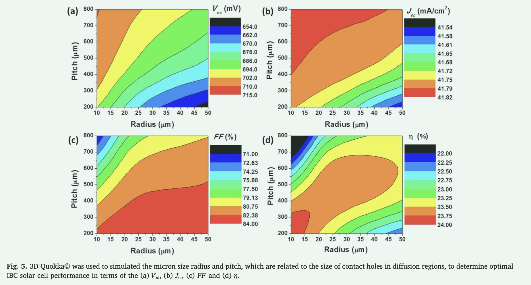
In this section, 3D Quokka@ simulation is used to simulate the Voc, Jsc, FF, and η of IBC solar cells with different contact ratios. The diffusion and passivation parameters of IBC solar cells are consistent with different contact ratios. The Rs values for n+ and p+ surfaces are 14 Ω/□ and 70 Ω/□, respectively. Table 1 lists the values for Jo,BSF, Jo,e, ρc-n+, and ρc-p+. As the contact ratio varies, the contact hole radius ranges from 10 μm to 50 μm, and the contact hole spacing ranges from 200 μm to 800 μm. Table 2 summarizes the simulation parameters for the design of the micron contact size of IBC solar cells. The values of Jo,cont-n+, Jo,cont-p+, and Jo,FSF are 570 fA/cm2, 1250 fA/cm2, and 15 fA/cm2, respectively. In the simulation of a micron-sized IBC solar cell, the BSF fraction for the rear was 0.12 and the body lifetime was 5 ms.
The values obtained using the parameters in Table 2 are shown in Figure 5a-d, where the radius and spacing represent the size of the contact holes and the distance of adjacent holes in the p+ emitter and n+ BSF regions, respectively. According to Figure 5a-d, Voc, Jsc, FF, and η differ with decreasing radius and spacing. The larger the spacing and the smaller the radius, the higher the Voc value, but the smaller the FF value. The smaller the pitch and the larger the radius, the smaller the Voc and the higher the FF. The reason for this is that, as can be seen in Figure 4, Jo decreases as the contact ratio decreases. These simulation results are consistent with equations (1)-(3) (Section 2.1) and indicate that the lower the Jo value, the higher the Voc value. Therefore, the size of the radius and spacing of the contact geometry should be balanced. The optimized (simulated) radius and spacing in Figure 5 increased the Voc by nearly 40.0 mV. The radius and spacing decreased from 50 μm and 200 μm to 10 μm and 200 μm, the FF decreased by nearly 10.0%, and the radius and spacing decreased from 10 μm and 800 μm to 10 μm and 200 μm, respectively. While a conversion efficiency of 23.5% is impressive, note that these values are based on 30 μm and 600 μm radii and spacing. Deposition conditions and passivation techniques can produce lower passivation parameters and high FF, which in principle can further improve η.

3.2. Explore IBC solar cells with micron-scale contact and fit-doping levels
The device was fabricated in a 3D Quokka@ using the Rs experimentally determined in Section 2.2 and the optimal spacing and contact hole radius values in Section 3.1.
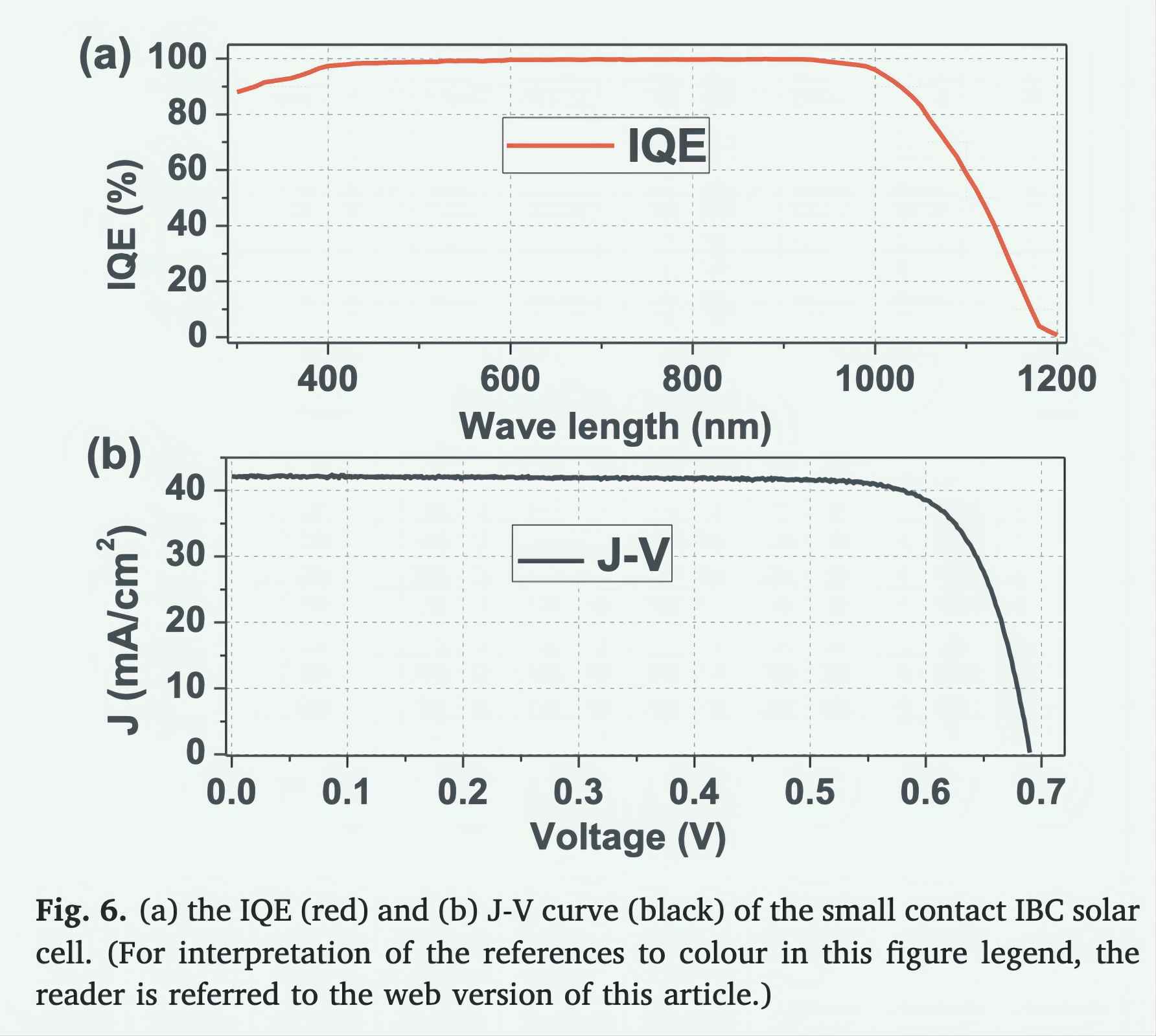
Figure 6a shows an internal quantum efficiency (IQE) image of an IBC solar cell with micron-scale contact and fit-doping levels. The lower absorption of the pre-SiNx:H layer improves IQE at smaller wavelengths. This suggests that the low reflection and high slew rate of the incident illumination result in a larger output current. The cell size is 2⨯2 cm2, the bulk resistivity is 3 Ω⨯cm, the pitch is 600 μm, and the contact radius is 30 μm, which is stable and can be obtained with low-cost industrial processing. The Rs values for n+ and p+ surfaces are 14 Ω/□ and 70 Ω/□, respectively.
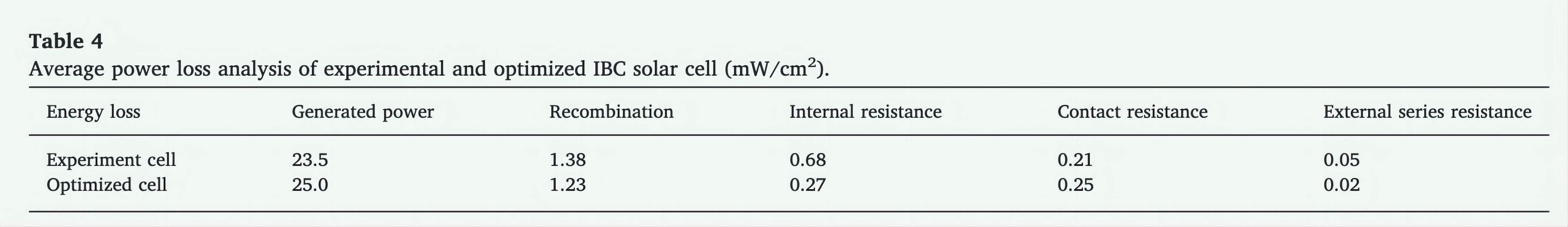
Figure 6b contains the J-V characteristics of a small-contact IBC solar cell at AM 1.5G. The solar cell η was 23.5%, the Voc was 690.0 mV, the Jsc was 42.0 mA/cm2, and the FF was 81.0%. Figure 5 shows that the simulated solar cells produce 692.5 mV, 41.8 mA/cm2 Jsc, 81.3% FF, and 23.5% η. Therefore, the experimental cell results are consistent with the simulated cells. The results show that IBC solar cells with micron-scale contacts can optimize the Jo value to produce relatively high Voc and η values according to the equation. (1)–(3).
3.3. Simulate the doping level of the optimized micron-contact IBC cell as a function of Rs
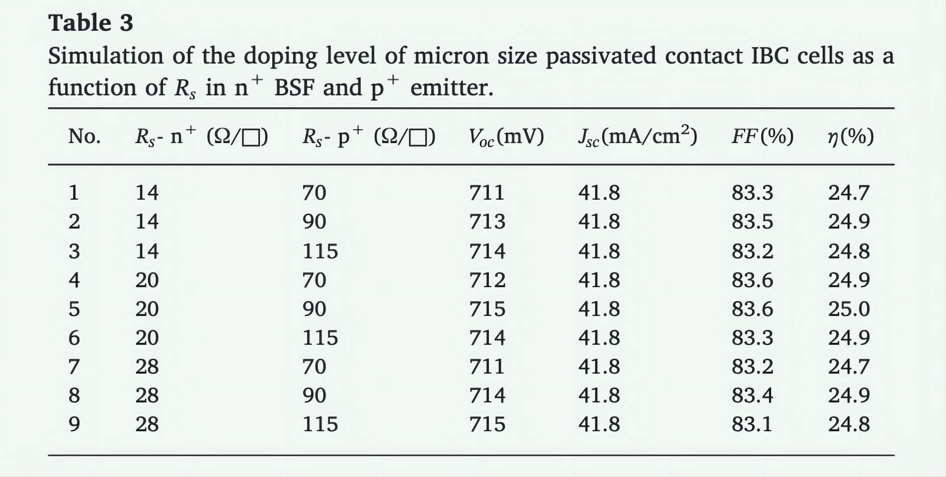
Table 3 shows the doping levels of Rs in the n+BSF and p+ emitters of micron-scale passivated contact IBC cells. The simulation uses a high volume-lifetime wafer, low contact resistance, and micron-level passivated contacts. The electron and contact pore radii are 100 μm and 5 μm, respectively, and the volume life is 9 ms. The BSF score in the rear dropped to 0.04. The reference device has re-transplanted Jo,FSF,Jo,cont-n+, and Jo,cont-p+ values of 5 fA/cm2, 280 fA/cm2, and 810 fA/cm2, respectively (Franklin et al., 2016). The other parameter values used are shown in Table 1. The results show that the performance of solar cells is improved by optimizing the doping level, high volume life wafers, and passivated contacts. The results show that the intermediate doping level, the Rs values of n+ BSF and p+ emitters are 20 Ω/□ and 90 Ω/□, respectively, and the passivation contact in the high volume life silicon wafer is ideal for achieving optimized IBC solar cells, with a Voc of 715 mV, Jsc of 41.8 mA/cm2, FF of 83.5%, and η of 25.0%.
3.4. Experimentally optimized power loss analysis of IBC solar cells
Table 4 shows the average power loss analysis of the experimental and optimized IBC solar cells. The energy loss is related to the current passing through the diffuser, through the contact interface, along the gate and busbar, and through the bottom of the battery. The external series resistor power loss of the optimized cell is 0.03 mW/cm2 smaller than that of the experimental cell. The combined power loss of the optimized solar cellis 0.15 mW/cm2, which is smaller than that of the experimental battery. The internal resistance power loss of the optimized solar cellis 0.41 mW/cm2, which is smaller than that of the experimental battery, while the contact resistance power loss of the optimized solar cellis 0.04 mW/cm2, which is greater than that of the experimental battery. As a result, the combined and internal resistance of the experimental cell resulted in a power loss of 0.56 mW/cm2 higher compared to the optimized cell. The power loss between these two cells may mainly come from the smaller micron size contact geometry and the optimized doping level.
The level of doping and micron-scale passivation contact in IBC solar cells has a large impact on the efficiency of IBC solar cells. With low contact resistivity metallization technology, micron-level passivation contacts and optimized doping levels can be achieved in wafers with high volume lifetime, resulting in lower Jo and improved FF and Vocof of cells.
4. Conclusion
Our study concludes that Jo and ρc are affected by doping levels, contact geometry, and passivation in IBC solar cells. For example, if the Rs value decreases, ρc can be reduced by an order of magnitude. Jo is also reduced by reducing the doping level. On the other hand, if Rs increases, the passivation of the BSF or Jo in the emitter region will decrease. The use of micron-scale passivation contact technology allows for optimal small-size contact geometry and reduces the overall Jo of the solar cell. Our method of fabricating IBC solar cells using micron-sized contact holes and special doping levels achieves efficiencies of up to 23.5%. A 3D Quokka@ was used to simulate the performance of IBC solar cells under various combinations of contact size, pitch and doping level. The efficiency of IBC solar cells can be significantly further improved through passivation contacts of micron size and spacing, low ρc and intermediate doping levels of junctions. We have developed a low-cost technology for industrial production. Based on the current design and hypothetical composite parameters, we predict that the IBC cell can reach an efficiency of 25.0%, a volume lifetime of 9 ms, a contact radius of 5 μm, a pitch of 100 μm, a Jo, FSF of 5 fA/cm2, and Rs values of 20 Ω/□ and 90 Ω/□ for n+ BSF and p+ emitter surfaces, respectively. In other words, the optimized micron-size passivation contact, doping level, and lower contact resistance minimize the Jo and ρc values, which provide superior IBC solar cell performance compared to traditional metallization and diffusion processes.


 English
 español
 한국의
한국의


 IPv6 network supported