

TOPCon solar cells with ultra-thin silicon oxide SiOx film and phosphorus-doped polysilicon Poly layer have a theoretical efficiency limit of up to 28.7%, becoming a hot research technology in the industry. TOPCon cells show superior passivation quality at the metal-silicon contact interface, with higher carrier selectivity and lower recombination rate. However, n+Poly layers of different thicknesses will affect the microstructure formed by the metallized contact, the passivation effect and the electrical performance of the cell.
Doped polysilicon is usually crystallized from an amorphous silicon layer a-Si after high temperature heat treatment. Typically, the preparation methods include PECVD, LPCVD, atmospheric pressure CVD, high pressure CVD, sputtering and electron beam evaporation. By studying the parameters of the passivation contact, such as the structural properties and thickness of the SiOx film and the Poly layer and the metallization of the passivation contact, it can provide valuable insights into the influence of the deposition preparation process parameters on the Poly layer and the cell performance.
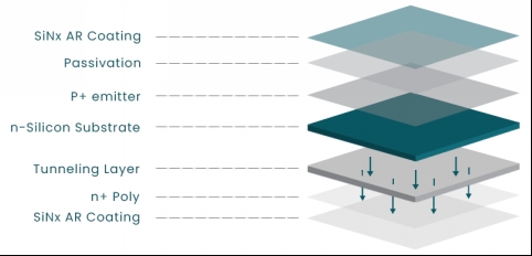
Schematic diagram of TOPCon solar cell structure
By controlling the interface defects of the SiOx film and the doping concentration of the Poly layer, the doped Poly layer can obtain good passivation performance and low contact resistivity. The thickness of the Poly layer can be changed by controlling the deposition process method. Different thicknesses will affect the saturation current density, metallization composite and contact resistivity ρc of the emitter.
Below we measure and analyze polysilicon Poly layers with thicknesses of 30nm, 50nm, 70nm, and 100nm.
Sheet resistance R□
When the thickness of the n+Poly layer decreases from 100nm to 30nm, the sheet resistance (R□) of the cell increases from 45.1 to 57.2Ω/sq. This is because the thickness of the Poly layer determines the total doping amount. Although the surface doping concentration is the same, as the thickness continues to increase, the total doping amount also increases, resulting in a decrease in the sheet resistance of the cell.
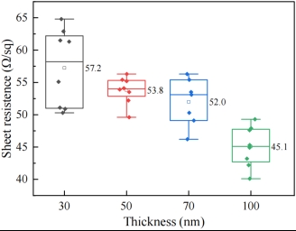
Sheet resistance diagram of TOPCon solar cells with different n+Poly layer thickness
Contact resistivity ρc
When the thickness of the n+Poly layer increases from 30nm to 100nm, the contact resistivity decreases significantly. As the thickness increases, the total doping concentration also increases, thereby narrowing the width of the depletion region inside the silicon wafer and promoting the quantum tunneling effect of carriers through the Schottky barrier. A thicker Poly layer can provide more doping atoms and reduce contact resistivity.
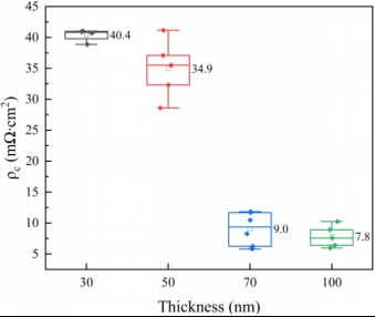
Contact resistivity ρc diagram of TOPCon solar cells with different n+Poly layer thickness
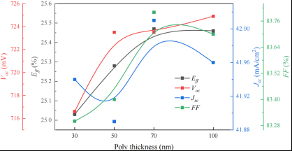
I-V parameters
The thinner n+Poly layer (30 nm) cannot provide sufficient doping concentration and passivation effect, resulting in lower efficiency Eff and open circuit voltage Voc. When the n+Poly layer thickness is 70 nm and 100 nm, the efficiency Eff, open circuit voltage Voc and fill factor FF of the solar cell are all optimal. This shows that these two thicknesses can provide good electrical performance and balanced doping concentration and resistance characteristics.
Table. I-V parameters of TOPCon solar cells with different n+Poly layer thicknesses
I-V parameters of TOPCon solar cells with different n+Poly layer thicknesses
From the above, it can be concluded that the thickness of the Poly layer has a significant impact on the electrical performance of TOPCon solar cells. Thicker Poly layers have lower sheet resistance and provide higher conductivity. This also shows that when designing and manufacturing solar cells, the thickness of the Poly layer needs to be optimized, which is critical to achieving high-efficiency TOPCon solar cells.


 English
 español
 한국의
한국의


 IPv6 network supported