

Crystalline silicon solar cells are one of the major solar cell technologies currently on the market, in which the metallization of silicon wafers plays a vital role in effectively collecting solar energy. The contact formation and characteristics between the silicon wafer and the metal gate line are affected by the doping level of the PN junction. The impact of the doping concentration on the cell performance can be judged by measuring the sheet resistance. The contact resistance between the cell and the metal gate line can be judged by measuring the quality of contact resistance. These tests play a leading role in improving solar cell performance. GT Solar can provide PV-Reflectometer, Contact Resistance Tester and (In-Line) Four Point Probe Tester to meet the testing needs of users, enabling precise control of various parameters of solar cells during the production process and providing customers with a variety of options.
Analysis of the influence of doping rate on solar cell surface reflectance
To create efficient crystalline silicon solar cells, optical surface reflections can be reduced by forming evenly distributed pyramid structures on the surface of the silicon wafer. The lower optical reflectivity mainly depends on the shape, size and uniformity of the pyramids on the silicon wafer surface. These pyramid structures are controlled by etch rate, potassium hydroxide (KOH), and isopropyl alcohol (IPA), where the etch rate affects the formation of pyramids, KOH affects the number of pyramids, and isopropyl alcohol affects the size of the pyramids.
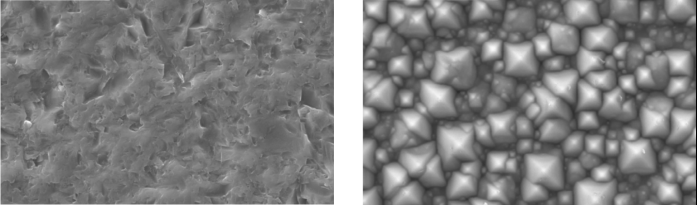
SEM images of original silicon wafer (left) and silicon wafer after cleaning and texturing process (right)
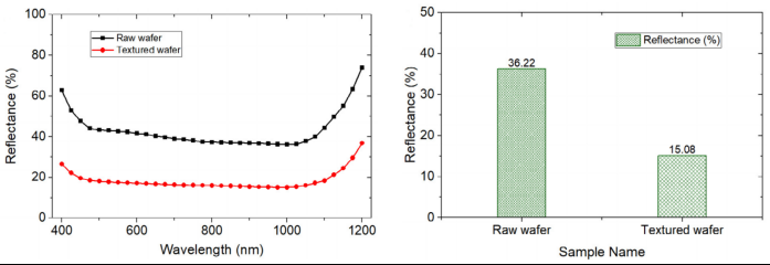
Comparison of reflectance versus wavelength curves (left) and reflectivity percentage (right) of original silicon wafers and silicon wafers after cleaning and texturing.
Analysis of the Effect of Doping Time on Film Sheet Resistance
In the photovoltaic industry, the sheet resistance of the film is critical to cell performance as it indicates the quality and uniformity of the PN junction doped area. A higher sheet resistance represents light doping, which will cause the silicon wafer contact resistance to be too high, while a low sheet resistance represents heavy doping, which will cause the silicon wafer contact resistance to be too low.
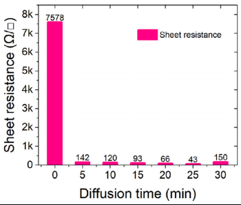
Changes in sheet resistance values of 5 groups of silicon wafers as diffusion time increases
It can be observed from the figure above that the sheet resistance value of silicon wafers doped with phosphorus atoms is significantly reduced. The sheet resistance before diffusion is 7578Ω/□. As the diffusion time increases, the sheet resistance values of the five groups of silicon wafers decrease rapidly until the value of sheet resistance is minimum at 25 minutes. This is because as the diffusion time increases, the doping concentration of phosphorus atoms also increases, and the sheet resistance value is inversely proportional to the doping concentration. At 30 minutes, the square resistance value began to increase again, which was due to over-doping.
Analysis of the influence of doping time on solar cell contact resistance
Contact resistance is affected by three main factors, namely semiconductor material, doping concentration and conductor material type. Doping concentration is an important factor in controlling contact resistance. Higher doping concentration will significantly reduce contact resistance. However, when the concentration of phosphorus atoms exceeds the solid solubility limit of the silicon wafer, a "dead layer" will be formed on the semiconductor surface. By rendering the silicon wafer electrically inactive, it also acts as a recombination center, hindering the conversion efficiency of the solar cell.
By doping six cell samples with phosphorus atoms respectively, the time changes were 5min, 10min, 15min, 20min, 25min and 30min respectively, and the contact resistance of the six areas on the front and back surfaces of the cell was measured.
Table 1. Front surface contact resistance values of 6 samples
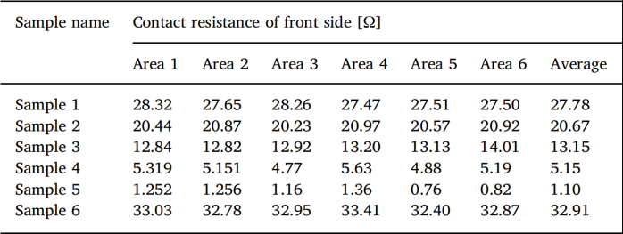
Table 2. Back contact resistance values of 6 samples
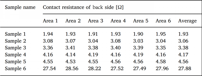
From the above two sets of data, it can be concluded that the contact resistance of the front surface decreases as the phosphorus doping time increases, but when it reaches 30 minutes, a "dead layer" is formed on the surface of the silicon wafer and the contact resistance value increases. The contact resistance value of the back surface is different from that of the front surface. It also increases slowly with the increase of doping time until it starts to rise sharply after 25 minutes. The reason may be that the solid solubility of phosphorus atoms in silicon wafers exceeds the limit.
Therefore, the diffusion time of 25 minutes can be regarded as the optimal time, which is beneficial to the production of high-efficiency crystalline silicon solar cells.
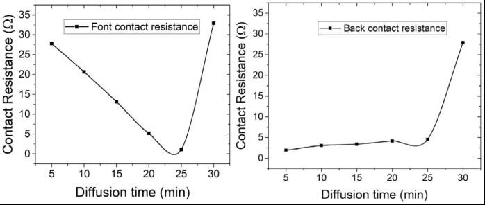
Contact resistance versus diffusion time curves for front (left) and back (right) solar cells


 English
 español
 한국의
한국의


 IPv6 network supported