This study solves the question of how the doped amorphous silicon layer in silicon heterojunction solar cells treated with hydrofluoric acid (HF) affects their performance. It was found that low concentrations (2.5-5.0%) of HF solutions had different effects on n-type and p-type amorphous silicon layers. In addition, HF exposure of n-type crystallite or p-type amorphous silicon layers correspondingly leads to the highest degradation of fill factor and short-circuit current. The situation is even worse for n-type amorphous silicon, where HF treatment leads to significant degradation of all solar cell parameters.
Today, silicon heterojunction (SHJ) solar cells exhibit the highest conversion efficiency among single-junction silicon solar cells [1], especially SHJ cells with interdigitated dorsal contacts (SHJ-IBC) [2]. Hydrofluoric acid (HF) is commonly used in the manufacture of SHJ solar cells for crystalline silicon (c-Si) wafer surface treatment, immediately before the plasma-enhanced chemical vapor deposition (PECVD) process. Its function is to remove natural oxides and provide hydrogen-terminated surface passivation, resisting contamination and oxidation in a short period of time. However, the fabrication of SHJ solar cells may result in doped amorphous (a-Si) or microcrystalline (mc-Si) silicon layers that may also be oxidized (e.g., due to an unexpected long-term PVD system shutdown). Therefore, the question now is whether a transient HF drop can improve the parameters of the SHJ solar cells in this case. Although there is literature on HF treatment of c-Si wafers [3-5], the question of how HF treatment doped with a-Si layer affects the parameters of SHJ solar cells remains well resolved [6].
In this work, to answer this question, we propose a simple method based on the use of a single-sided PECVD silicon nitride (SiNx) mask layer that protects the doped layer and intrinsic amorphous silicon layer underneath during HF exposure. It should be mentioned that this issue is also most closely related to the fabrication of SHJ-IBC solar cells, where HF is used for surface cleaning and/or etching of SiNx or SiOx sacrificial layers [7, 8].
Three types of SHJ structures were used in this work (schematic diagram shown in Figure 1): 1) standard n/i/c-Si/i/p structure (type A), 2) and 3) identical n/i/c-Si/i/p structure with n layer (type B) or p-layer (type C) coated with a 100 nm thick SiNx layer. The SHJ structure is based on textured, 6", CZ, n-type c-Si wafers with the same 1Ωcm resistivity and 150μm thickness. The n-layer is either a-Si or mc-Si, while the p-layer is always a-Si. As mentioned above, the purpose of the SiNx layer on the front or back is to protect the underlying non-silicon layer during HF immersion. In all three cases, the parameters of the eigenlayer and the doped a-Si and SiNx layers are the same. The SiNx and a-Si layers were deposited by RF plasma discharge at 13.56 MHz and 40.68 MHz at a substrate temperature of 200 °C, respectively.

In order to minimize the effects of other processes, such as wet chemical texturing and cleaning, the effects of sputtering deposition (PVD) of PECVD, indium tin oxide (ITO) layers, and screen printing of silver contact grids on the experimental results, we used a pilot line for SHJ cells in our R&D center [9]. Therefore, in each process step, the wafers are processed simultaneously. Before sputtering depositing the ITO layer, additional HF treatment is used at room temperature. HF-treated wafers are exposed to air for no more than 20 minutes. SHJ solar cells have a rear emitter, bifacial, busbar-less design. The calibrated GridTOUCH system [10] is used to measure the current-voltage characteristics of the solar cell under standard test conditions (1000 W/m2 irradiance, AM1.5 spectrum, and 25°C solar cell temperature).
Results discussed
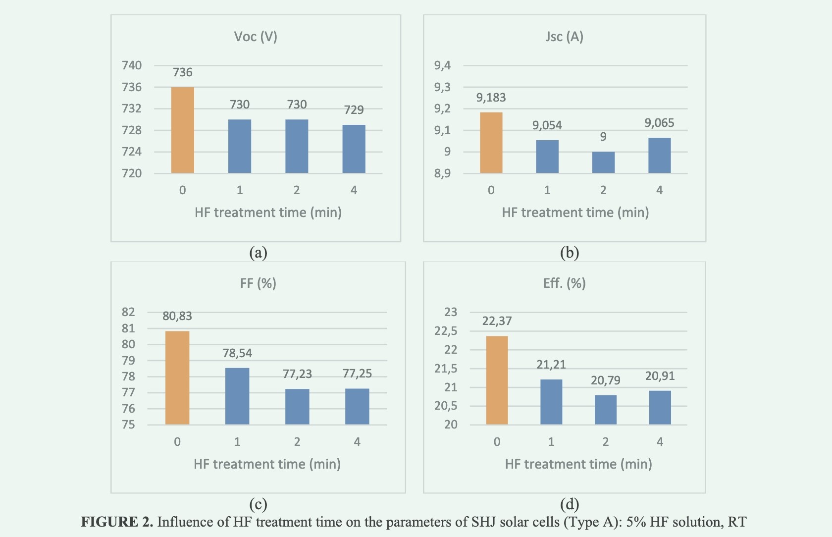
First, we investigated how HF treatment of p-type and n-type layers prior to ITO layer deposition affects the performance of SHJ solar cells. In this case, 24 identical wafers (type A with n-mc-Si layers) are processed simultaneously in wet chemistry and PECVD processes and then divided into four equal groups (8 wafers each). Figure 2 shows the average parameters for each group of SHJ solar cells with different HF treatment durations prior to ITO layer deposition. For comparison, the parameters of SHJ cells not immersed in the doped layer in HF are shown (first orange column). It can be seen that the conversion efficiency of SHJ solar cells decreased from the initial 22.37% to 21.21%, that is, the average abs decreased by 1.16% after 1 minute of 5% HF treatment on the two doped layers. This rapid degradation is followed by a slow degradation phase on a longer time scale. The decrease in efficiency here is caused by the deterioration of all solar cell parameters. In this case, a longer HF immersion (up to 10 minutes, not shown here) resulted in a slightly lower performance of the SHJ solar cell.
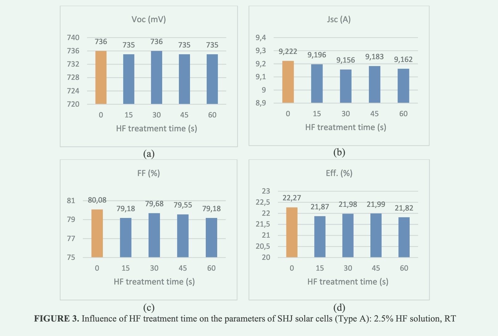
It is well known that natural oxides on textured n-type c-Si wafers can be removed in 5% HF solution within 30 s. For this reason, the same experiment is then repeated on a shorter time scale (1 min) using HF solution at twice the lower concentration (2.5%). In this case, a small decrease in cell efficiency (0.4% absolute) was observed, which was already observed after the first 15 sec of HF exposure, as shown in Figure 3. Unlike in the past, the efficiency drop is now mainly caused by the deterioration of the short-circuit current (JSC) and fill factor (FF), while the open-circuit voltage (VOC) remains almost constant. However, in both cases, the degradation kinetics are similar, including both fast and slow phases, as described above. Interestingly, the time dependence is similar to the etching rate of c-Si in HF solution. However, in the latter case, the time scale is much longer (10s-100s days) [4]. A simple explanation for this behavior is that the hydrogenated a-Si surface contains a large number of dangling bonds. During the fast phase, the passivation of the catenary bond by hydrogen in the aqueous HF solution [15] slows down the etching rate on longer time scales.
Secondly, to answer the question of which doped a-Si layer is more affected by HF, B-type and C-type samples have been prepared. In this case, the HF treatment time (3 min) was chosen to be approximately equal to the etching time of the 100 nm thick SiNx layer. Table 1 shows the parameters of the SHJ solar cell, where the n-layer (type C) or p-layer (type B) is mainly exposed to HF prior to the deposition of the ITO layer. For comparison, the parameters of SHJ solar cells (type A) that are not immersed in HF are also shown in the table.

 Table 1.3 min Effect of HF treatment of n-layer or p-layer on SHJ solar cell parameters.2.5% high-frequency solution, room temperature.

It can be seen that HF has different effects on the n-layer and the p-a-Si layer. Therefore, the fill factor is most affected by the HF-treated n-mc-Si layer, while the short-circuit current degradation is the most abundant for the HF-treated p-a-Si layer. There is also a slight change in the open-circuit voltage of the n-mc-Si and p-a-Si layers treated by HF. However, for SHJ cells with HF treatment with n-a-Si layers, the worst-case scenario was observed, with a significant deterioration of all cell parameters after HF treatment. HF exposure of the n-a-Si layer compared to the n-mc-Si and p-a-Si layers also results in a wide range of variations in cell parameters within the group (see the last row of Table I, showing the upper and lower limits).

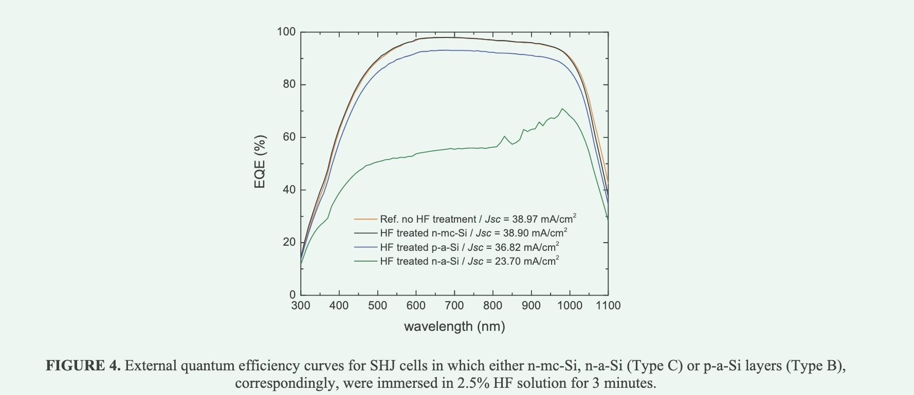
Figure 4 shows the external quantum efficiency of SHJ cells based on Type B and Type C samples, respectively. The EQE curves (orange) of SHJ cells based on an A-type structure without HF treatment are also shown here for comparison. It can be seen that 3 min exposure to 2.5% HF in the n-type microcrystalline silicon layer has little effect on the external quantum efficiency of the cell. There is only a small blue shift, which is most likely indicative of a decrease in the thickness of the n mc-Si layer. On the other hand, when the p-type amorphous silicon layer is immersed in the same HF solution, the EQE is significantly reduced across the wavelength range. For HF-treated n-type amorphous silicon layers, a further reduction in EQE was observed. These results show that the n-mc-Si, p-a-Si, and n-a-Si layers have different etching rates (ERs) in the diluted HF solution.
In general, n-type semiconductors are known to have more filled states in the band gap and are therefore chemically more reactive than p-type semiconductors and have higher etch rates [11]. For example, Lui and colleagues [3] recently discovered an unexpected etching rate (0.8 nm/min) of n-type c-Si with high doping (carrier concentration> 1020 cm-3) in diluted HF. However, the etching properties of a-Si:H films are more complex than c-Si because the hydrogen content and bonding configuration can vary, and because they are irregularly structured. Our results show that ER(n-a-Si)> ER(n-mc-Si)> ER (p-a-Si) are consistent with KOH and dry etching of doped a-Si films in a diluted HF solution [12,13]. The etch rate of n-mc-Si is smaller compared to n-a-Si, which may be due to the fact that n-mc-Si also contains a c-Si fraction, while the etch rate of c-Si in HF is usually low or insignificant[4]. In addition, n-mc-Si has a different hydrogen content compared to n-a-Si [14]. However, the question of why EQE deteriorates significantly in the case of HF-treated pa-Si layers remains open and warrants further investigation.
Conclusion
A simple method based on a single-sided PECVD SiNx masking layer has been applied to examine the effect of HF-treated doped a-Si layers on the performance of SHJ cells. It was found that the diluted HF solution had less negative effects on the n-mc-Si and p-a-Si layers in SHJ cells, but not on the n-a-Si layers, due to the difference in etch rates. Therefore, brief HF immersion of SHJ cells with highly oxidized n-mc-Si and p-a-Si layers may help to improve their performance. However, HF concentrations and treatment duration should be minimal. Our results also show that n mc-Si is more suitable than n-a-Si for SHJ-IBC cell fabrication, where post-contact patterning is performed using a wet chemical process.