Silicon solar cells can generally be divided into monocrystalline, polycrystalline and amorphous silicon solar cells, of which monocrystalline silicon cells are currently the fastest developed solar cells, its structure and production process has been finalized, and is widely used in space and ground.In this issue, we will introduce you to the boron diffusion process of n-type monocrystalline silicon cells!
Boron diffusion process principle
The principle of boron diffusion process is to prepare a p-n junction by boron diffusion in the preparation process of n-type monocrystalline silicon cells, forming a p-n junction. The boron-doped n-type silicon wafer is diffused at high temperature through the liquid source of boron tribromide, so that the liquid boron oxide is deposited on the surface of the silicon wafer in the diffusion furnace tube, and the reduction reaction with Si is formed to form boron oxide, and the boron oxide is used as a diffusion source to diffuse to the inside of the silicon wafer at high temperature to form a pn junction. In the process of atmospheric pressure boron diffusion, the boiling point of boron oxide, the reaction product, is above 1600 °C, and it is always in a liquid state during the diffusion process, which can only be diluted and dispersed to the surface of silicon wafers with a large amount of nitrogen, and the diffusion uniformity is difficult to control. The method of deep oxidation after diffusion can effectively reduce the dead layer and improve the uniformity of the p-n junction.

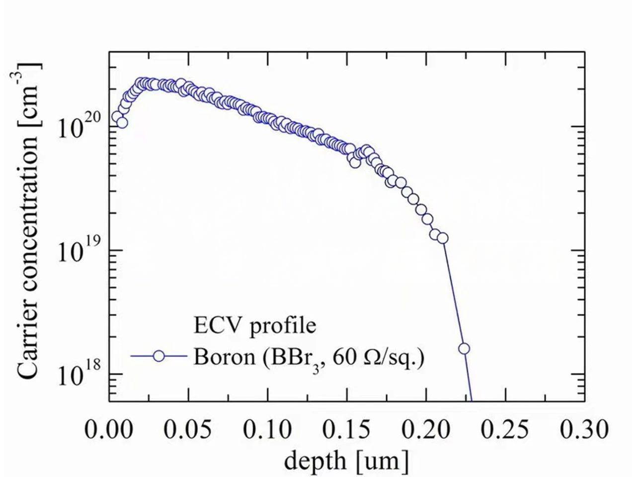
Diffusion map of boron on zone-melted monocrystalline silicon
Boron diffusion background technology
For the boron diffusion process, not only the boron content in the prepared p-n junction has an important impact on the resistivity and square resistance of n-type monocrystalline silicon cells, but also the uniformity of boron diffusion also affects the resistivity and square resistance of the solar cell
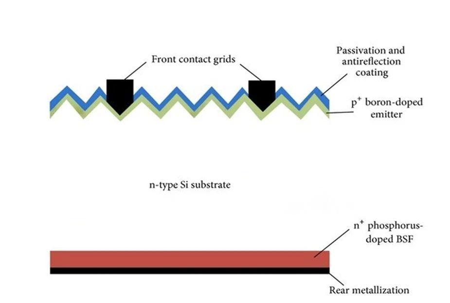
 Schematic diagram of an N-type silicon wafer doped with boron
In order to ensure the resistivity and square resistance of n-type monocrystalline silicon cells, the boron content in n-type monocrystalline silicon cells is generally controlled to prevent the boron content from being too high, so as to increase the square resistance. However, in the prior art, when reducing the boron content and increasing the square resistance, it is often easy to have uneven distribution of boron sources, resulting in uneven distribution of boron content in a single monocrystalline silicon cell, resulting in the resistivity of a certain part of the monocrystalline silicon cell being too high, thereby affecting the photoelectric conversion rate of the cell. And with the increase of production and the increase of silicon wafer size, the non-uniformity of boron content is more obvious.
The diffusion indicator determines the degree of diffusion
The diffusion index is mainly expressed by the square resistance, junction depth and surface concentration of the solar cell, among which the square resistance value is mainly the comprehensive characterization of the surface concentration and junction depth, which has an important impact on the parameters of the solar cell, and the diffusion p-n junction depth will directly affect its absorption of short-wave light. The shallower the diffusion p-n junction over a certain range, the higher the square resistance value and the higher the current value. Generally speaking, within a certain range, the greater the diffusion concentration, the greater the open-circuit voltage.