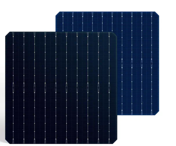
1.Texturing
The texturing section (a total of 6 lines) includes pre-cleaning - pure water washing before texturing - texturing *3 - pure water washing after texturing - post-cleaning - pure water washing after cleaning - pickling - pure water washing after pickling - slow lifting pre-dehydration - drying *5 and other modules.
1) Pre-cleaning purpose: to remove impurities (organic matter and metal impurities, etc.) adhered to the surface of the silicon wafer, using NaOH solution and H2O2 solution.
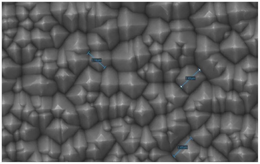
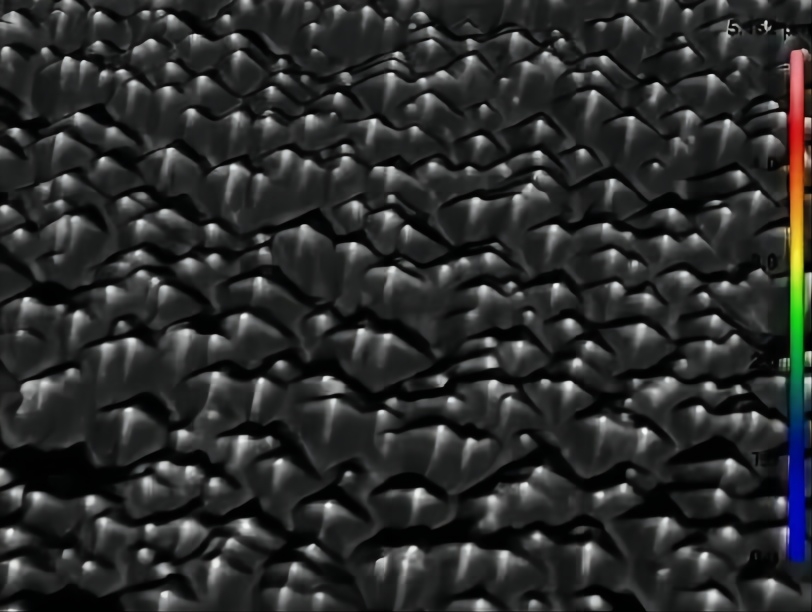
2) The purpose of alkali velvet making: the anisotropic corrosion of the silicon surface is carried out by lye to form a pyramid with a surface size of 5um, and the pyramid suede has excellent light trapping and anti-reflection effect (10%). Alkaline texturing uses NaOH solution and texturing additives.
3) The silicon wafer after alkali texturing is cleaned and enters the post-cleaning tank to remove the residual organic matter and ensure the cleanliness of the surface of the silicon wafer, so as to improve the conversion efficiency of the cell to a certain extent.
4) After pickling, it is necessary to use dilute acid solution (3.15% HCl and 7.1% HF) for high-purity cleaning, the function of HCl is to neutralize the residual NaOH, and the function of HF is to remove the oxide layer on the surface of the silicon wafer to make the surface of the silicon wafer more hydrophobic, forming the complex of silicon H2SiF6, which separates the metal ions from the surface of the silicon wafer through complexation with metal ions, so that the metal ion content of the silicon wafer is reduced, and prepares for diffusion knotting. Pickling is followed by pure water cleaning.
5) Purpose of slow lifting pre-dehydration: pre-dehydration of the surface of crystalline silicon wafers, usually as the last step of pure water cleaning. The crystalline silicon wafer cleaned with pure water is transferred to the slow drawing tank, the silicon wafer is first immersed in pure water and completely immersed, and then slowly lifted upwards through the manipulator and hanging basket, and the surface tension can pull down the water film on the silicon wafer.
6) Drying: The wafer is transferred to the drying tank, and the hot air at 90°C is blown up and down to the wafer for drying, and the drying adopts electric heating.
2 Boron diffusion
The purpose of the diffusion process is to form a PN junction on a silicon wafer to realize the conversion of light energy into electrical energy. The PN junction manufacturing equipment is a diffusion furnace, and the project uses gaseous boron trichloride to diffuse the silicon wafer in the diffusion furnace, and the boron atoms enter the silicon wafer through diffusion, and at the same time form a borosilicate glass layer on the surface of the silicon wafer.
3 SE laser redoping

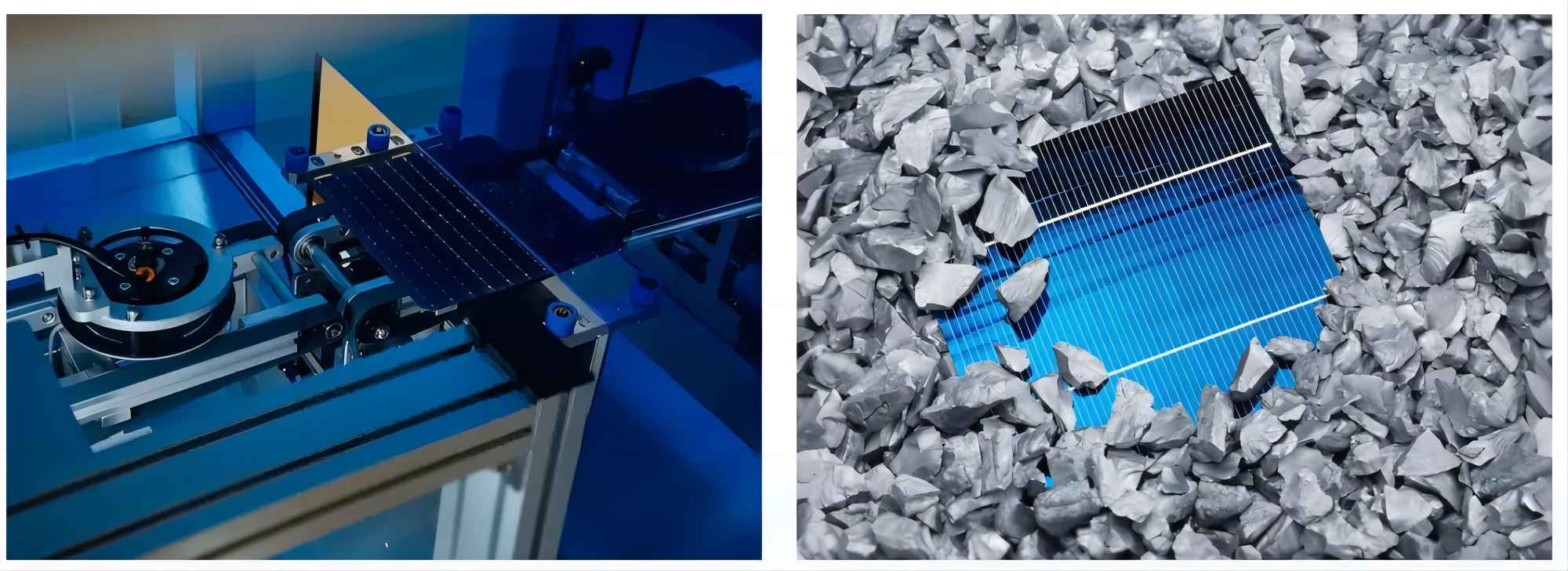
Laser doping technology is to perform heavy doping on the contact part of the metal grid (electrode) with the silicon wafer, while maintaining light doping (low-concentration doping) outside the electrode.
4 Post-oxidation
Where the surface of the silicon wafer has been treated by laser SE, the oxide layer of the boron diffusion surface (the in-light surface) is destroyed by the laser spot energy. In alkali polishing etching, an oxide layer is required as a masking layer to protect the phosphorus diffusion surface of the silicon wafer (into the glossy surface). Therefore, oxide repair is required on the surface scanned by the laser SE.
4.Etching
1) Remove BSG: The silicon wafer is removed from the BSG on the back side by floating on water in a chain cleaning machine (the back side is in contact with acid), and the main component of the acid is 24.5% HF.
2) Back etching: In order to improve the reflectivity of the back side of the silicon wafer, the back side of the silicon wafer is polished by alkali plus polishing agent. The alkali polishing section (6 lines) includes pre-cleaning, water washing, alkali polishing *2-hydrogen peroxide cleaning (reserved) - micro-texturing (reserved) - pure water cleaning - post-cleaning - pure water cleaning - pickling *2 - pure water washing after pickling - slow lifting and pre-dehydration - drying *5 and other modules.
3) The pre-cleaned processed silicon wafer enters the cleaning tank to remove the residual organic matter and ensure the cleanliness of the silicon wafer surface, so as to improve the cell conversion efficiency to a certain extent.
4) The alkali blasting tank is equipped with pure water, and an appropriate amount of NaOH solution and polishing additives are added (NaOH solution is about 1.6%, and the polishing agent concentration is 0.97%), and then the back surface of the silicon wafer is polished at an operating temperature of 65 °C. After alkali washing, pure water cleaning is carried out.
5) Add pure water to the post-cleaning and micro-making trough, and add an appropriate amount of NaOH solution and hydrogen peroxide (about 0.55% NaOH solution, hydrogen peroxide concentration 0.25%) according to the ratio for room temperature cleaning. After cleaning, clean with pure water.
6) After pickling, it is necessary to use dilute acid solution (0.9% HCl and 0.23% HF) for high-purity cleaning, the role of HCl is to neutralize the residual NaOH, and the function of HF is to remove the oxide layer on the surface of the silicon wafer to make the surface of the silicon wafer more hydrophobic, forming a complex of silicon H2SiF6, and detaching the metal ions from the surface of the silicon wafer through complexation with metal ions, so that the metal ion content of the silicon wafer is reduced, and preparation for diffusion bonding. Pickling is followed by pure water cleaning.
7) Drying: The crystalline silicon wafer after slow lifting and pre-dehydration is transferred to the drying tank, and the hot air at 90°C is blown up and down to the silicon wafer for drying, and the drying is electrically heated.
5 POPAID deposition in situ doping
The POPAID process is a key process for the preparation of plate coatings by integrating tunneling oxide layers and doped crystalline silicon layers.
First, the silicon wafer enters the loading chamber in the atmospheric environment, is transmitted to the preheating chamber at 300°, and then enters the PO process cavity, at this time, O2 is transported to the gas separator block through the air pipe, and the ionization is activated by the RF radio frequency power supply into ions, and the ions are oxidized on the surface of the silicon wafer to form a tunneling oxide layer; Buffer cavity, transmitted into the paid cavity, the paid source deposits a certain thickness of amorphous silicon on the back of the substrate, and at the same time passes PH3 gas into the deposition process, and the gaseous phosphine enters the machine, and the phosphorus in the phosphine is excited into the state of phosphorus ions by 10kev and 0.5-2kev high-voltage radio frequency, and the direct current high voltage is added between the ion source and the ground, so that the phosphorus ions obtain energy through the high-voltage electric field, the width of the beam is 420mm, and then the silicon wafer is transmitted to the lower part of the beam, and the atoms of the paid source fly to the substrate to carry P ions or react with P ions to achieve in-situ phosphorus doping.
6 .Annealing
The silicon wafer is placed in a reaction tube made of quartz glass, and the reaction tube is heated at a certain temperature with a resistance wire heating furnace (the commonly used temperature is 900~1200 °C, and it can be reduced to below 600 °C under special conditions), and when oxygen passes through the reaction tube, a chemical reaction occurs on the surface of the silicon wafer: Si (solid) + O2 (gaseous) → SiO2 (solid)
The redistribution of impurities generated during the annealing process also plays a role in absorbing impurities, and the adsorption and fixation of sodium and potassium ions by PSG are used to remove these harmful ions. Analysis of pollution production links: The main pollution links in this process are residual oxygen and nitrogen in the thermal oxygen link.
7.BOE cleaning
The BOE (5-line) trough equipment is an integrated semi-enclosed equipment, and the silicon wafers are placed in the basket by the automation equipment and converted in each tank solution in the equipment through the robotic arm. Among them, the chemical tank is continuously replenished with corresponding chemicals according to the concentration of the solution, and the whole is replaced regularly. The replaced waste liquid is discharged into the wastewater system and finally into the sewage treatment station for treatment.
1) Pickling: dilute acid solution (3.15% HCl and 7.1% HF) for high-purity cleaning, the role of HCl is to use Cl-complex metal ions, the role of HF is to remove the oxide layer on the surface of the silicon wafer to make the surface of the silicon wafer more hydrophobic, the formation of silicon complex H2SiF6, through the complexation of metal ions and metal ions will be separated from the surface of the silicon wafer, so that the metal ion content of the silicon wafer is reduced, HF pickling 150s to remove the front BSG and the back of the PSG layer, pickling after pure water cleaning.
2) After pickling, it is necessary to use dilute acid solution (14.7% HF) for high-purity cleaning after post-cleaning, the function of HF is to remove the oxide layer on the surface of the silicon wafer to make the surface of the silicon wafer more hydrophobic, forming a complex of silicon H2SiF6, and detaching the metal ions from the surface of the silicon wafer through complexation with metal ions, so that the metal ion content of the silicon wafer is reduced.
3) Drying: The crystalline silicon wafer after slow lifting and pre-dehydration is transferred to the drying tank, and the hot air at 90°C is blown up and down to the silicon wafer for drying, and the drying adopts electric heating.
8. ALD
ALD equipment is used to coat the surface of the silicon wafer with an Al2O3 layer to improve the passivation and impurity absorption effect on the surface of the silicon wafer. It mainly uses gaseous Al(CH3)3 to react with water vapor (H2O) to generate Al(OH)3, which adheres to the surface of silicon wafers and produces methane gas at the same time.
9. Front-side coating
The basic principle is to use high-frequency optical discharge to generate plasma to exert influence on the deposition process of thin films, promote the decomposition, compounding, excitation and ionization of gas molecules, and promote the formation of reactive groups. Since the presence of NH3 is conducive to the flow and diffusion of active groups, the growth rate of the film is increased, and the deposition temperature is greatly reduced.
10. Back coating
The PECVD back membrane equipment is a closed negative pressure equipment, electric heating, and comes with an oil-free dry mechanical vacuum pump. During production, the equipment is first filled with nitrogen, the robotic arm completes the loading of silicon wafers, and after the external pressure is reached in the equipment, the inlet and outlet are opened, and the graphite boat automatically enters the equipment and closes the inlet and outlet.
Vacuuming and various safety inspections are carried out, and after confirming the safety, silane and ammonia are introduced to complete the silicon nitride coating in the equipment. After the coating is completed, the residual gas in the special gas pipeline and equipment is discharged through nitrogen, and then the inlet and outlet are opened and discharged. After cooling, it enters the finishing and enters the subsequent process.
11. Metallization
1) During the printing process, the slurry is above the screen, and the scraper is pressed on the screen with a certain pressure, so that the screen is deformed and contacts the surface of the silicon wafer. The slurry is extruded and comes into contact with the surface of the silicon wafer, and the surface of the silicon wafer has a large adsorption force, snatching the slurry out of the mesh.
2) Sintering is to sinter the main fine grid slurry printed on the silicon wafer into a cell at a high temperature, so that the electrode is embedded in the surface to form a firm mechanical contact and a good electrical connection, and finally the electrode and the silicon wafer itself form an ohmic contact.
3) After the sintering of the electrically injected cell, the method of direct electrical injection of carriers (reverse injection of direct current) is used to change the charged state of hydrogen in the silicon body, so that the boron-oxygen complex in the attenuation state can be well passivated, so that it can be transformed into a stable re-ecology, and finally achieve the purpose of anti-light decay.
12 Test Packaging
