Diffusion process -sheet resistance
Oct 30, 2023
Definition
- Sheet resistance
- Refers to the resistance of a semiconductor film or a metal film per unit area
- Sheet resistance is only related to film thickness and material properties

- R-resistance -Ω, ρ- resistivity Ω.cm, L-length -cm, S- area -cm²
- Rs=ρ/d
- Rs-sheet resistance -Ω/sq, ρ- resistivity -Ω.cm, d- thickness -cm
Linear four probe test principle
- Four probes with equal spacing of S
-
- The probe applies appropriate pressure and falls vertically on the silicon wafer to form ohmic contact
- A current (I) is applied between the two outer probes (1,4) to form a test loop
- Two intermediate probes (2,3) are connected to a high-impedance precision voltmeter and the potential difference V is measured


When the sample diameter is greater than 40s, the thickness is d>5s, the edge effect correction factor and thickness correction factor are both 1, the resistivity calculation formula:
ρ=2πsV/I
For extremely thin samples, the thickness (W) is much smaller than the probe spacing (s) (w/s<0.5), when the horizontal dimension is infinite:

- In the case of equidistant probe test, the probe spacing is independent of the measured result, and the resistivity is proportional to the thickness (W) of the measured sample
- 4.5324 - often referred to as sheet resistance correction factor
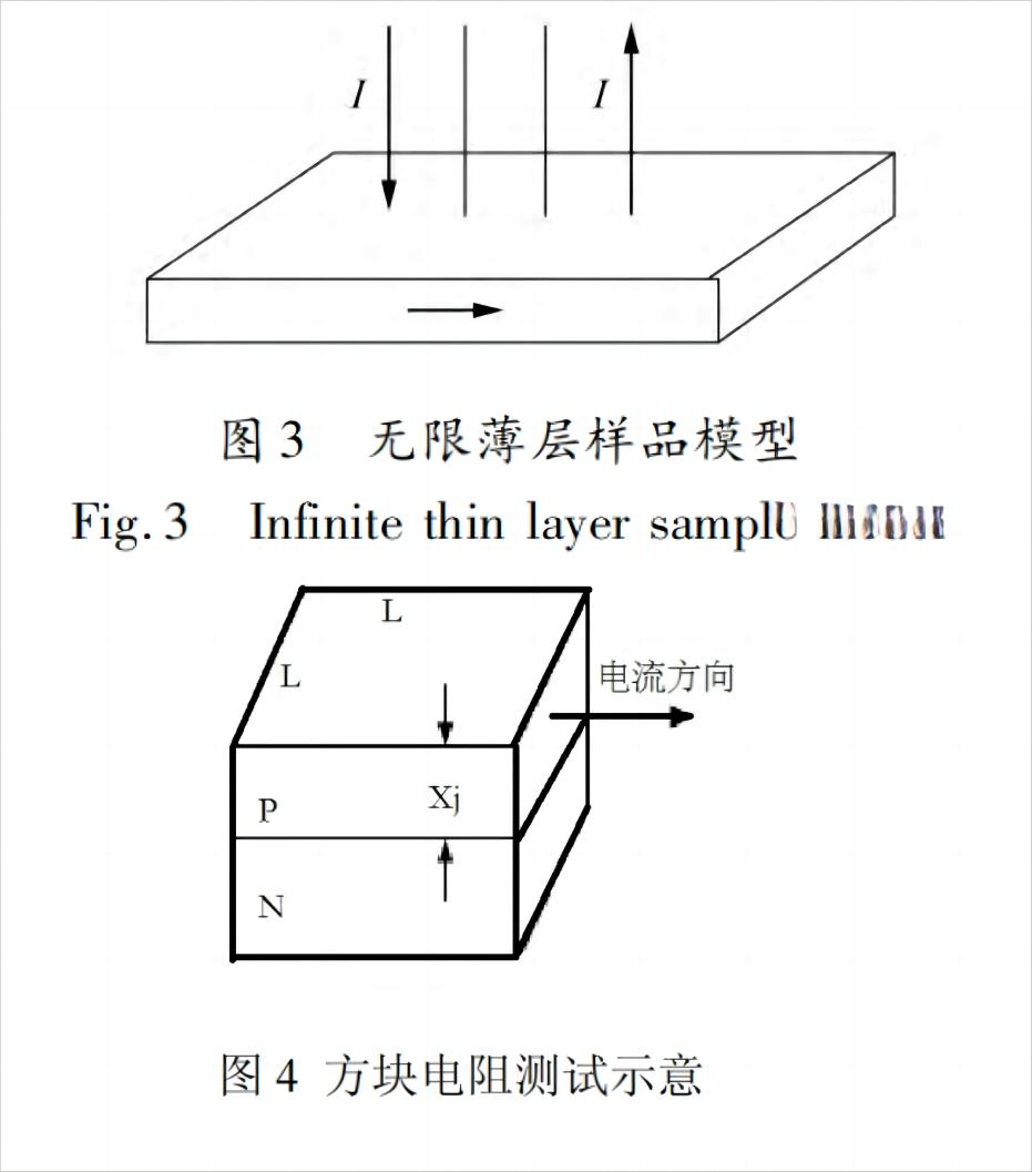
Sheet resistance, a thin layer of semiconductor with a square surface, showing resistance in the direction of current
- Rs=ρ/Xj=4.5324V23/I
- Xj,Junction depth
Advantages and disadvantages of linear four probe method:
Advantages:
- The test theory is simple and mature, and it is reliable after practical test.
- The test accuracy is higher than that of other probe methods under the same conditions.
- There are no strict requirements on the size of the test wafer, and it can be used to test wafers with irregular shapes or thicknesses.
disadvantage
- Contact testing, prone to damage or contaminate the wafer under test.
- The test needs to form a stable ohmic contact, and the test time is long, especially when testing multiple points.
- Contact testing requires higher wafer contact surfaces.
Conversion of doping concentration and resistivity
For P-type silicon

- ρ-resistivity,N-Doping concentration
For N-type silicon


 English
 español
 한국의
한국의


 IPv6 network supported